XC6VLX75T-1FFG484C
High-performance Virtex-6 FPGA with 74496 cells, 484-pin FCBGA
Manufacturer: xilinx
series introduction
# Introduction to the XC6VLX75T - 1FFG484C Product Series
## 1. Overview
The XC6VLX75T - 1FFG484C belongs to the Xilinx Virtex - 6 family of Field - Programmable Gate Arrays (FPGAs). FPGAs are semiconductor devices that can be programmed and reprogrammed by the user after manufacturing, offering a high degree of flexibility and adaptability for a wide range of applications. This particular model, with its unique combination of features and specifications, is designed to meet the demanding requirements of modern electronic systems.
## 2. Key Features
### 2.1 Logic Resources
- **Logic Cells**: The XC6VLX75T - 1FFG484C is equipped with a substantial number of logic cells. These cells are the building blocks of digital circuits and can be configured to implement various functions such as arithmetic operations, data storage, and control logic. The large number of logic cells allows for the implementation of complex algorithms and systems on a single chip.
- **Slice Architecture**: It uses a slice - based architecture. Each slice contains look - up tables (LUTs), flip - flops, and carry logic. LUTs can be used to implement any Boolean function of a given number of inputs, while flip - flops are used for sequential logic. The carry logic enables efficient implementation of arithmetic operations like addition and subtraction.
### 2.2 Memory Resources
- **Block RAM**: The FPGA has a significant amount of block RAM. Block RAMs are large, pre - fabricated memory blocks that can be used for data storage, buffering, and implementing functions such as FIFOs (First - In - First - Out) and dual - port memories. This is particularly useful in applications where large amounts of data need to be stored and accessed quickly, such as in image and video processing.
- **Distributed RAM**: In addition to block RAM, it also has distributed RAM. Distributed RAM is formed by the LUTs in the slices and is suitable for small - scale memory requirements, providing a more flexible and fine - grained memory solution.
### 2.3 I/O Resources
- **High - Speed I/O**: The XC6VLX75T - 1FFG484C offers a variety of high - speed I/O interfaces. These interfaces support different communication protocols such as PCI Express, Ethernet, and Serial RapidIO. High - speed I/O is crucial for applications that require fast data transfer between the FPGA and external devices, such as in networking equipment and high - performance computing systems.
- **I/O Standards**: It supports a wide range of I/O standards, including LVCMOS, LVDS, and SSTL. This allows the FPGA to interface with different types of external devices, providing compatibility with a diverse set of systems.
### 2.4 DSP Resources
- **DSP Slices**: The FPGA contains dedicated DSP slices. These slices are optimized for performing digital signal processing operations such as multiplication, addition, and filtering. The presence of DSP slices makes the XC6VLX75T - 1FFG484C well - suited for applications in areas like audio and video processing, wireless communication, and radar systems.
### 2.5 Power Management
- **Low - Power Design**: Xilinx has incorporated advanced power - management techniques in the XC6VLX75T - 1FFG484C. It offers multiple power - saving modes, allowing the user to optimize the power consumption of the FPGA according to the application requirements. This is especially important in battery - powered devices and energy - efficient systems.
## 3. Package and Pinout
The "FFG484" in the product name refers
Images for reference
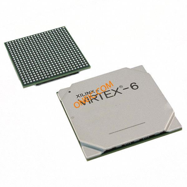
Virtex 6 LXT Series
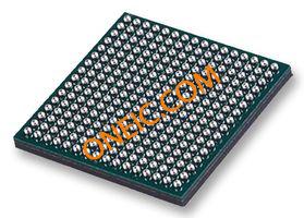
Image Preview
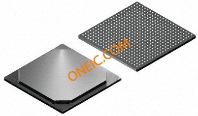
Image Preview