XC6VLX130T-2FFG784I
High-performance FPGAs with 784-pin FCBGA for advanced electronic systems
Manufacturer: xilinx
series introduction
# Introduction to the XC6VLX130T - 2FFG784I Product Series
## 1. Overview
The XC6VLX130T - 2FFG784I belongs to the Xilinx Virtex - 6 FPGA (Field - Programmable Gate Array) product family. FPGAs are integrated circuits that can be programmed and reprogrammed by the user after manufacturing, offering a high degree of flexibility and customization for a wide range of applications. This particular model, with its specific configuration, is designed to meet the demanding requirements of various industries, including telecommunications, industrial automation, and high - performance computing.
## 2. Key Features
### 2.1 Logic Capacity
The XC6VLX130T - 2FFG784I offers a substantial logic capacity. It contains a large number of configurable logic blocks (CLBs), which are the basic building blocks of an FPGA. These CLBs can be used to implement complex digital circuits, such as arithmetic units, state machines, and data path elements. The high logic capacity allows designers to integrate multiple functions onto a single chip, reducing the overall system cost and board space.
### 2.2 Speed Grade
The “- 2” in the part number indicates the speed grade of the FPGA. A higher speed grade generally means that the device can operate at faster clock frequencies, enabling it to handle high - speed data processing tasks. This is crucial for applications such as high - speed data communication, where data needs to be processed and transmitted in real - time.
### 2.3 Package Type
The “FFG784” refers to the package type of the XC6VLX130T - 2FFG784I. It is a Fine - Pitch Ball Grid Array (FBGA) package with 784 pins. The FBGA package offers several advantages, including good thermal performance, high pin density, and mechanical stability. The high pin density allows for a large number of input/output (I/O) connections, which is essential for interfacing with external components such as memory chips, sensors, and communication interfaces.
### 2.4 I/O Capabilities
This FPGA provides a rich set of I/O options. It supports a variety of I/O standards, such as LVCMOS (Low - Voltage Complementary Metal - Oxide - Semiconductor), LVDS (Low - Voltage Differential Signaling), and SSTL (Stub Series Terminated Logic). These I/O standards enable the FPGA to interface with different types of external devices, including high - speed serial interfaces, memory modules, and general - purpose I/O devices.
### 2.5 Embedded Memory
The XC6VLX130T - 2FFG784I includes embedded Block RAM (BRAM) and Distributed RAM. The BRAM is organized into large memory blocks, which can be used for storing data, such as buffers for data streaming applications. The Distributed RAM, on the other hand, is distributed throughout the FPGA fabric and can be used for smaller - scale data storage and temporary data handling.
### 2.6 DSP Slices
It is equipped with a significant number of Digital Signal Processing (DSP) slices. These DSP slices are optimized for performing high - speed arithmetic operations, such as multiplication, addition, and accumulation. They are particularly useful for applications in digital signal processing, such as audio and video processing, wireless communication, and radar systems.
## 3. Applications
### 3.1 Telecommunications
In the telecommunications industry, the XC6VLX130T - 2FFG784I can be used for a variety of tasks. It can be used to implement high - speed data interfaces, such as Ethernet, Fibre Channel, and Serial
Images for reference
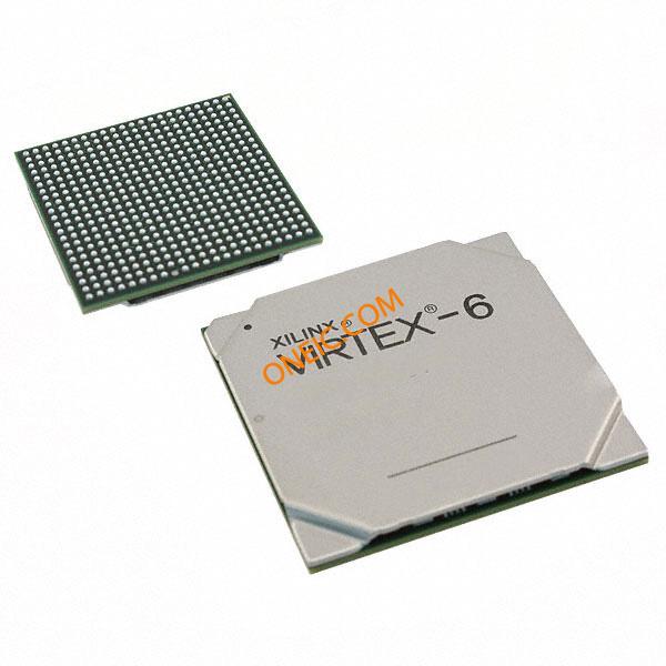
Virtex 6 LXT Series