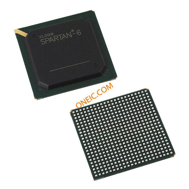
XC6SLX45-2FGG676I
High-performance FPGA chips with 676-pin FBGA for advanced electronics
Manufacturer: xilinx
series introduction
# Introduction to the XC6SLX45 - 2FGG676I Product Series
## 1. Overview
The XC6SLX45 - 2FGG676I belongs to the Spartan - 6 family of Field - Programmable Gate Arrays (FPGAs) developed by Xilinx. FPGAs are integrated circuits that can be programmed and reprogrammed by the user after manufacturing, offering a high degree of flexibility for a wide range of applications. This particular model, with its specific configuration, is designed to meet the needs of various industries, including telecommunications, industrial automation, and consumer electronics.
## 2. Key Features
### 2.1 Logic Capacity
The XC6SLX45 - 2FGG676I provides a substantial amount of logic resources. It has approximately 45,000 logic cells, which are the basic building blocks for implementing digital circuits. These logic cells can be used to create complex combinational and sequential logic functions, such as arithmetic circuits, state machines, and data processing units. This high logic capacity allows designers to integrate multiple functions onto a single FPGA, reducing the need for multiple discrete components and simplifying the overall system design.
### 2.2 Speed Grade
The “- 2” in the part number indicates the speed grade of the FPGA. A higher speed grade generally means that the device can operate at faster clock frequencies and has shorter propagation delays. The XC6SLX45 - 2FGG676I with a speed grade of 2 is suitable for applications that require high - speed data processing and real - time operation, such as high - speed communication interfaces and high - performance signal processing.
### 2.3 Package Type
The “FGG676” refers to the package type of the FPGA. It is a Fine - Pitch Ball Grid Array (FBGA) package with 676 pins. The FBGA package offers several advantages, including a high pin count, which allows for a large number of input and output signals to be connected to the FPGA. It also provides good thermal performance due to the large surface area of the package, which helps in dissipating heat generated during operation. Additionally, the fine - pitch design enables a more compact PCB layout, saving board space.
### 2.4 I/O Resources
This FPGA has a rich set of Input/Output (I/O) resources. It supports a variety of I/O standards, such as LVCMOS (Low - Voltage Complementary Metal - Oxide - Semiconductor), LVDS (Low - Voltage Differential Signaling), and SSTL (Stub Series Terminated Logic). This wide range of I/O standards makes it compatible with different types of external devices, such as microcontrollers, memory chips, and communication interfaces. The large number of I/O pins also allows for easy interfacing with multiple external components, enabling the FPGA to be used in complex system designs.
### 2.5 Embedded Memory
The XC6SLX45 - 2FGG676I includes embedded Block RAM (BRAM) and Distributed RAM. The BRAM provides large - capacity, high - speed memory storage, which can be used for buffering data, implementing FIFO (First - In - First - Out) queues, and storing configuration data. The Distributed RAM, on the other hand, is used for smaller - scale memory requirements and can be integrated directly into the logic fabric of the FPGA. This combination of embedded memory resources enhances the data - handling capabilities of the FPGA and enables efficient implementation of memory - intensive applications.
### 2.6 Digital Signal Processing (DSP) Slices
It is equipped with a number of DSP slices. These DSP slices are optimized for performing high - speed arithmetic operations, such as multiplication, addition, and
Images for reference
Spartan 6 LX