XC6SLX16-3CPG196I
High-performance FPGA chips with 196-pin CSBGA for advanced electronics
Manufacturer: xilinx
series introduction
# Introduction to the XC6SLX16 - 3CPG196I Product Series
## 1. Overview
The XC6SLX16 - 3CPG196I belongs to the Spartan - 6 family of Field - Programmable Gate Arrays (FPGAs) developed by Xilinx. FPGAs are integrated circuits that can be programmed and reprogrammed by the user after manufacturing, offering a high degree of flexibility for a wide range of applications. This particular product in the series is designed to provide a balance between performance, cost, and power consumption, making it suitable for various embedded and industrial applications.
## 2. Key Features
### 2.1 Logic Resources
- **Slice Count**: The XC6SLX16 - 3CPG196I offers a significant number of logic slices. These slices are the basic building blocks of the FPGA and can be configured to implement combinational and sequential logic functions. With a sufficient number of slices, it can handle complex digital designs, such as state machines, arithmetic circuits, and data processing units.
- **Look - Up Tables (LUTs) and Flip - Flops**: Each slice contains LUTs and flip - flops. LUTs are used to implement Boolean functions, while flip - flops are used for storing data. The combination of these elements allows for the implementation of both simple and complex digital circuits, enabling designers to create custom logic for their specific applications.
### 2.2 Memory Resources
- **Block RAM**: It is equipped with block RAM modules. These large - scale memory blocks can be used for various purposes, such as buffering data, implementing FIFO (First - In - First - Out) queues, and storing configuration data. The block RAM provides high - speed access to data, which is crucial for applications that require fast data processing and storage.
- **Distributed RAM**: In addition to block RAM, the FPGA also has distributed RAM. Distributed RAM is smaller in size but can be more flexibly configured. It is often used for storing small amounts of data or implementing local memory within a logic circuit.
### 2.3 I/O Resources
- **I/O Pins**: The XC6SLX16 - 3CPG196I comes with a set of I/O pins that can be configured to support different I/O standards. These standards include LVCMOS (Low - Voltage Complementary Metal - Oxide - Semiconductor), LVDS (Low - Voltage Differential Signaling), and others. This flexibility allows the FPGA to interface with a wide variety of external devices, such as sensors, actuators, and communication interfaces.
- **I/O Banks**: The I/O pins are organized into banks, which can be independently powered and configured. This feature provides isolation and flexibility in power management and signal integrity, making it easier to interface with different voltage levels and types of external devices.
### 2.4 Performance
- **Speed Grade**: The “3” in the part number indicates the speed grade of the FPGA. A higher speed grade generally means that the FPGA can operate at higher clock frequencies, resulting in faster data processing and better overall performance. This makes the XC6SLX16 - 3CPG196I suitable for applications that require high - speed data transfer and real - time processing.
- **Clock Management**: It has built - in clock management resources, such as Phase - Locked Loops (PLLs) and Delay - Locked Loops (DLLs). These components are used to generate and control the clock signals within the FPGA, ensuring accurate timing and synchronization of the digital circuits.
### 2.5 Power Consumption
- **Low - Power Design**: Xilinx has designed the Spartan - 6 family, including the XC6SL
Images for reference
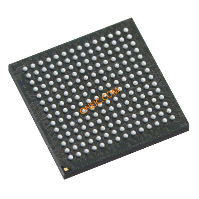
196-TFBGA, CSBGA