XC6SLX16-2FTG256I
Compact Spartan-6 LX FPGAs for advanced electronic designs
Manufacturer: xilinx
series introduction
# Introduction to the XC6SLX16 - 2FTG256I Product Series
## 1. Overview
The XC6SLX16 - 2FTG256I belongs to the Spartan - 6 family of Field - Programmable Gate Arrays (FPGAs) developed by Xilinx. FPGAs are semiconductor devices that can be programmed after manufacturing, offering a high degree of flexibility and reconfigurability for a wide range of applications. This particular product in the series is designed to provide a balance between performance, cost, and power consumption, making it suitable for various embedded and industrial applications.
## 2. Key Features
### 2.1 Logic Resources
- **Slice Count**: The XC6SLX16 - 2FTG256I is equipped with a significant number of logic slices. These slices are the basic building blocks of the FPGA and can be configured to implement combinational and sequential logic functions. With a sufficient number of slices, it can handle complex digital designs, such as state machines, arithmetic circuits, and data processing units.
- **Look - Up Tables (LUTs) and Flip - Flops**: Each slice contains LUTs and flip - flops. LUTs are used to implement Boolean functions, while flip - flops are used for storing data. The combination of these elements allows for the implementation of both simple and complex digital circuits, enabling designers to create custom logic for their specific applications.
### 2.2 Memory Resources
- **Block RAM**: It has on - chip block RAMs that can be used for data storage and buffering. These block RAMs are organized in a way that allows for efficient data access, making them suitable for applications such as video buffering, data caching, and FIFO (First - In - First - Out) implementations.
- **Distributed RAM**: In addition to block RAM, the FPGA also has distributed RAM, which is formed by the LUTs in the logic slices. Distributed RAM can be used for smaller - scale data storage requirements and can be configured in different ways to meet the design needs.
### 2.3 I/O Resources
- **I/O Standards**: The XC6SLX16 - 2FTG256I supports a wide range of I/O standards, including LVCMOS (Low - Voltage Complementary Metal - Oxide - Semiconductor), LVDS (Low - Voltage Differential Signaling), and others. This allows it to interface with different types of external devices, such as microcontrollers, sensors, and communication modules.
- **I/O Pins**: With 256 pins in the FTG package, it provides a sufficient number of I/O pins for connecting to multiple external components. The I/O pins can be configured as input, output, or bidirectional, depending on the requirements of the application.
### 2.4 Performance
- **Speed Grade**: The “- 2” in the part number indicates the speed grade of the FPGA. A higher speed grade generally means that the FPGA can operate at higher clock frequencies, resulting in faster data processing and better overall performance. This makes it suitable for applications that require high - speed data transfer and real - time processing.
- **Clock Management**: It has built - in clock management resources, such as Phase - Locked Loops (PLLs) and Delay - Locked Loops (DLLs). These resources can be used to generate and distribute stable clock signals throughout the FPGA, ensuring proper synchronization of different parts of the design.
### 2.5 Power Consumption
- **Low - Power Design**: Xilinx has designed the Spartan - 6 family, including the XC6SLX16 - 2FTG256I, with low - power consumption in mind. This is
Images for reference
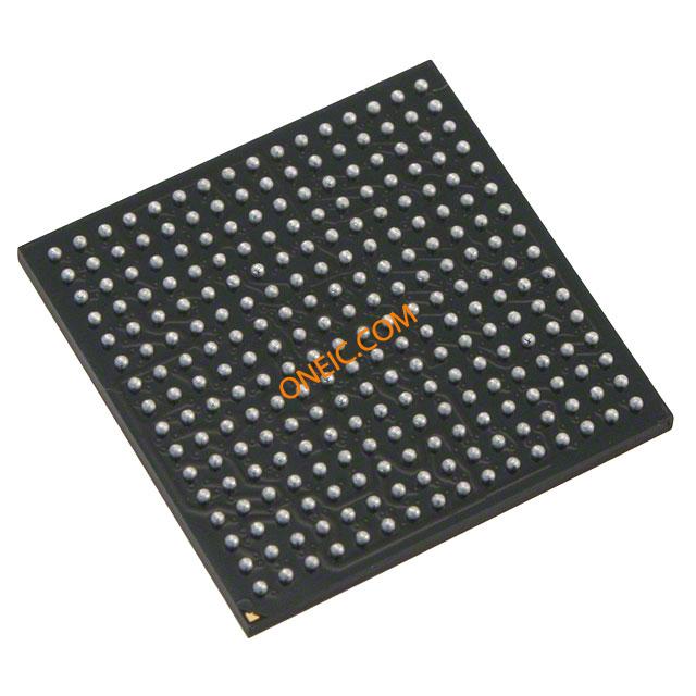
XC6SLX16-2FTG256I
Image Preview