XC6SLX150-L1FGG484I
High-performance FPGA chips with multiple I/O and advanced CMOS technology
Manufacturer: xilinx
series introduction
# Introduction to the XC6SLX150 - L1FGG484I Product Series
## 1. Overview
The XC6SLX150 - L1FGG484I belongs to the Spartan - 6 family of Field - Programmable Gate Arrays (FPGAs) developed by Xilinx. FPGAs are integrated circuits that can be programmed and reprogrammed by the user after manufacturing, offering a high degree of flexibility for a wide range of applications. The XC6SLX150 - L1FGG484I is designed to provide a balance between performance, cost, and power consumption, making it suitable for various industrial, communication, and consumer electronics applications.
## 2. Key Features
### 2.1 Logic Resources
- **Logic Cells**: The XC6SLX150 - L1FGG484I is equipped with a large number of logic cells. These cells are the basic building blocks of the FPGA and can be configured to implement various digital logic functions such as combinational logic (e.g., adders, multipliers) and sequential logic (e.g., flip - flops, registers). With a significant number of logic cells, it can handle complex digital designs, including those for signal processing, control systems, and data manipulation.
- **Slice Architecture**: It uses a slice - based architecture. Each slice contains a set of look - up tables (LUTs), flip - flops, and carry logic. LUTs are used to implement arbitrary Boolean functions, and the flip - flops store the state of the circuit. The carry logic is used for efficient arithmetic operations, enabling fast addition and subtraction.
### 2.2 Memory Resources
- **Block RAM**: The FPGA has a substantial amount of block RAM. Block RAMs are large, pre - fabricated memory blocks that can be used for data storage, buffering, and implementing memory - intensive functions such as FIR filters, video frame buffers, and data caches. They can be configured in different sizes and modes, providing flexibility for different application requirements.
- **Distributed RAM**: In addition to block RAM, it also has distributed RAM. Distributed RAM is formed by the LUTs in the logic slices and is useful for small - scale memory requirements, such as storing configuration data or small arrays.
### 2.3 I/O Resources
- **I/O Standards**: The XC6SLX150 - L1FGG484I supports a wide range of I/O standards, including LVCMOS, LVDS, and SSTL. This allows it to interface with different types of external devices, such as microcontrollers, memory chips, and communication interfaces. The ability to support multiple I/O standards makes it a versatile choice for system integration.
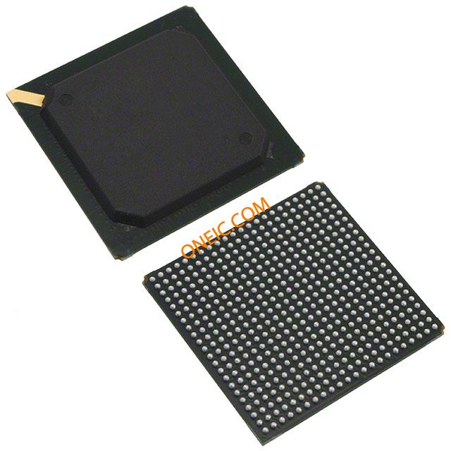
- **I/O Pins**: It has a total of 484 pins in the FGG package. These pins can be used for input and output signals, power supply, and ground connections. The large number of I/O pins provides sufficient connectivity for complex systems with multiple external components.
### 2.4 Clock Management
- **PLLs and DLLs**: The FPGA includes Phase - Locked Loops (PLLs) and Delay - Locked Loops (DLLs). PLLs are used to generate multiple clock signals with different frequencies, phases, and duty cycles from a single input clock. DLLs are used to control the delay of clock signals, which is important for synchronizing different parts of the circuit. The clock management resources ensure stable and accurate clocking for the entire system.
### 2.5 Power Management
- **Low - Power Operation**: The XC6SLX150 - L1FGG484I is designed with power - saving features. It has different power
Images for reference
XC6SLX25T-2FGG484C