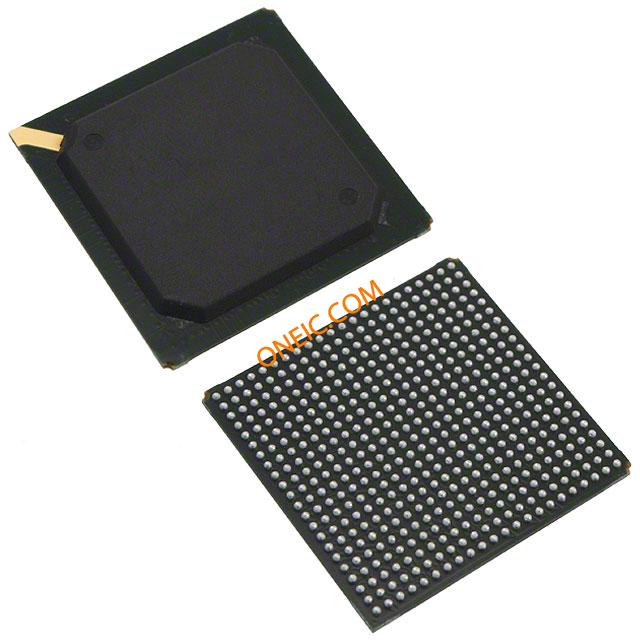
XC6SLX100-3FGG484I
High-density FPGA chips with 484-pin FBGA for advanced electronics
Manufacturer: xilinx
series introduction
# Introduction to the XC6SLX100 - 3FGG484I Product Series
## 1. Overview
The XC6SLX100 - 3FGG484I belongs to the Spartan - 6 family of Field - Programmable Gate Arrays (FPGAs) developed by Xilinx. FPGAs are integrated circuits that can be programmed and reprogrammed by the user after manufacturing, offering a high degree of flexibility for a wide range of applications. This particular model, with its specific configuration, is designed to meet the requirements of various industries, including telecommunications, industrial automation, and consumer electronics.
## 2. Key Features
### 2.1 Logic Capacity
The XC6SLX100 - 3FGG484I offers a significant amount of logic resources. It has approximately 100,000 equivalent logic cells, which can be used to implement complex digital circuits such as state machines, arithmetic units, and control logic. This high logic capacity allows designers to integrate multiple functions onto a single FPGA, reducing the need for multiple discrete components and thus saving board space and cost.
### 2.2 Speed Grade
The “- 3” in the part number indicates the speed grade of the FPGA. A higher speed grade generally means that the device can operate at faster clock frequencies and has shorter propagation delays. This is crucial for applications that require high - speed data processing, such as high - speed serial communication interfaces and real - time signal processing.
### 2.3 Package Type
The “FGG484” refers to the package type of the XC6SLX100 - 3FGG484I. It is a Fine - Pitch Ball Grid Array (FBGA) package with 484 pins. The FBGA package offers several advantages, including good thermal performance due to its large surface area for heat dissipation, and high pin density, which enables more input/output (I/O) connections. This makes it suitable for applications that require a large number of external connections, such as multi - channel data acquisition systems.
### 2.4 I/O Resources
This FPGA provides a rich set of I/O pins, which can be configured to support a variety of standard interfaces. It can support different voltage levels and signaling standards, such as LVCMOS (Low - Voltage Complementary Metal - Oxide - Semiconductor), LVDS (Low - Voltage Differential Signaling), and SSTL (Stub Series - Terminated Logic). This flexibility allows the XC6SLX100 - 3FGG484I to interface with a wide range of external devices, including microcontrollers, memory chips, and sensors.
### 2.5 Embedded Memory
The XC6SLX100 - 3FGG484I includes on - chip embedded memory blocks. These memory blocks can be used for various purposes, such as data buffering, storing configuration data, and implementing small - scale memories. The embedded memory helps in reducing the need for external memory chips, which simplifies the system design and improves the overall performance.
### 2.6 DSP Slices
It also features Digital Signal Processing (DSP) slices. These slices are optimized for performing high - speed arithmetic operations, such as multiplication, addition, and accumulation. They are particularly useful for applications in digital signal processing, such as audio and video processing, wireless communication, and radar systems.
## 3. Applications
### 3.1 Telecommunications
In the telecommunications industry, the XC6SLX100 - 3FGG484I can be used for tasks such as baseband processing in wireless communication systems. It can handle high - speed data streams, perform error correction coding, and implement modulation and demodulation algorithms. Additionally, it can be
Images for reference
XC6SLX25T-2FGG484C
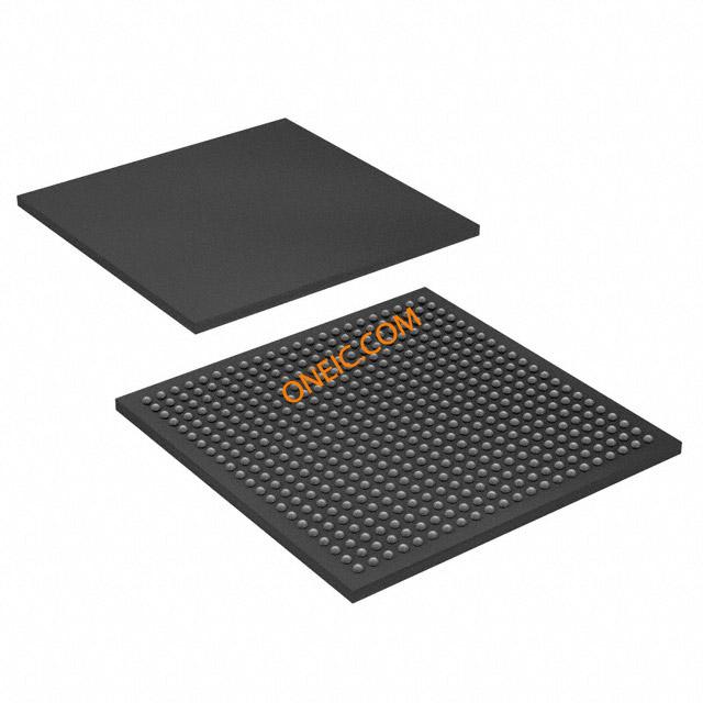
484-FBGA