XC5VLX50T-1FFG1136C
High-performance Virtex-5 FPGAs with 1136-pin FCBGA for advanced applications
Manufacturer: xilinx
series introduction
# Introduction to the XC5VLX50T - 1FFG1136C Product Series
## 1. Overview
The XC5VLX50T - 1FFG1136C belongs to the Xilinx Virtex - 5 LX field - programmable gate array (FPGA) product series. FPGAs are semiconductor devices that can be configured by a customer or a designer after manufacturing. This particular model offers a high - performance, flexible, and cost - effective solution for a wide range of applications, from telecommunications and networking to industrial control and high - end consumer electronics.
## 2. Key Features
### 2.1 Logic Resources
- **Slice Architecture**: The XC5VLX50T - 1FFG1136C is equipped with a large number of logic slices. These slices are the basic building blocks of the FPGA, containing look - up tables (LUTs) and flip - flops. The LUTs can implement any Boolean function of a certain number of inputs, while the flip - flops are used for sequential logic operations. This rich logic resource allows designers to implement complex digital circuits, such as state machines, arithmetic units, and data processing pipelines.
- **Logic Cell Count**: It has a significant number of logic cells, which provides the capacity to handle large - scale designs. This makes it suitable for applications that require high - density logic implementation, such as high - speed data processing and complex algorithm execution.
### 2.2 Memory Resources
- **Block RAM**: The device includes block random - access memory (BRAM) modules. These BRAMs are large, pre - fabricated memory blocks that can be used for various purposes, such as data buffering, FIFO (First - In - First - Out) queues, and small - scale data storage. The BRAM can be configured in different sizes and data widths, providing flexibility for different memory requirements in the design.
- **Distributed RAM**: In addition to block RAM, there is also distributed RAM available. Distributed RAM is formed by using the LUTs in the logic slices as memory elements. It is useful for small - scale, low - latency memory applications, such as storing configuration data or small lookup tables.
### 2.3 I/O Resources
- **High - Speed I/O**: The XC5VLX50T - 1FFG1136C features a large number of high - speed input/output (I/O) pins. These I/O pins support a variety of standard interfaces, including LVDS (Low - Voltage Differential Signaling), PCI Express, and Gigabit Ethernet. The high - speed I/O capabilities enable the device to communicate with external components at high data rates, making it suitable for applications that require fast data transfer, such as high - speed networking and data acquisition systems.
- **I/O Standards Support**: It supports a wide range of I/O standards, which allows for seamless integration with different types of external devices. This flexibility in I/O standards makes it easier for designers to interface the FPGA with other components in the system, reducing the complexity of the overall design.
### 2.4 DSP Resources
- **DSP Slices**: The product series includes dedicated digital signal processing (DSP) slices. These DSP slices are optimized for performing high - speed arithmetic operations, such as multiplication, addition, and accumulation. They are particularly useful for applications that require real - time signal processing, such as audio and video processing, wireless communication, and radar signal processing.
- **High - Performance DSP**: The DSP slices in the XC5VLX50T - 1FFG1136C offer high - performance capabilities, with fast clock speeds and low latency. This enables designers to implement complex DSP algorithms efficiently, improving the overall performance of the system.
## 3
Images for reference
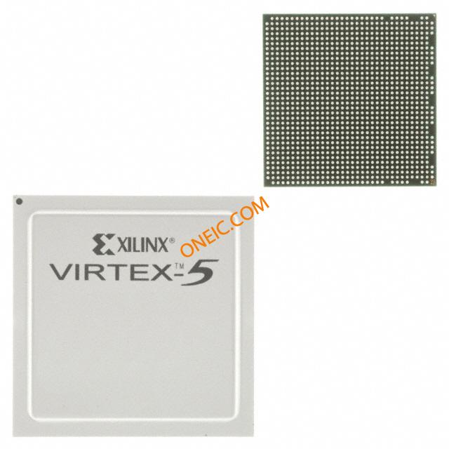
Xilinx- 1136-FBGA
Image Preview
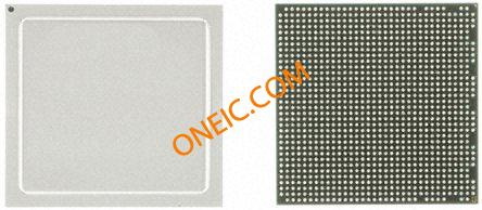
Image Preview