XC5VLX50-1FFG324C
High-density Virtex-5 LX FPGAs for advanced digital applications
Manufacturer: xilinx
series introduction
# Introduction to the XC5VLX50 - 1FFG324C Product Series
## 1. Overview
The XC5VLX50 - 1FFG324C belongs to the Xilinx Virtex - 5 LX field - programmable gate array (FPGA) product series. FPGAs are semiconductor devices that offer high - performance, flexible, and reconfigurable solutions for a wide range of applications. The XC5VLX50 - 1FFG324C is designed to meet the demanding requirements of modern electronic systems, providing a balance between logic capacity, performance, and power consumption.
## 2. Key Features
### 2.1 Logic Resources
- **Slice Count**: The XC5VLX50 - 1FFG324C is equipped with a significant number of logic slices. These slices are the basic building blocks of the FPGA, containing look - up tables (LUTs), flip - flops, and carry logic. The ample slice count allows for the implementation of complex digital circuits, such as state machines, arithmetic units, and data processing pipelines.
- **Distributed RAM**: It has on - chip distributed RAM resources. Distributed RAM can be used to store small amounts of data close to the logic elements, reducing the need for external memory access and improving the overall system performance. This is particularly useful for applications that require fast access to small data buffers, such as FIR filters and small - scale data caches.
### 2.2 Block RAM
- **Capacity**: The device features a large amount of block RAM. Block RAMs are larger, dedicated memory blocks that can be configured in various ways, such as single - port, dual - port, or simple dual - port memories. With a substantial block RAM capacity, the XC5VLX50 - 1FFG324C can handle large - scale data storage requirements, making it suitable for applications like video buffering, image processing, and data logging.
- **Flexible Configuration**: The block RAMs can be easily configured to meet different application needs. For example, they can be used to implement FIFOs (First - In - First - Out) buffers, which are essential for data flow management in communication systems and streaming data applications.
### 2.3 Digital Signal Processing (DSP) Slices
- **High - Performance DSP**: The XC5VLX50 - 1FFG324C includes a number of DSP slices. These slices are optimized for performing high - speed arithmetic operations, such as multiplication, addition, and accumulation. They are ideal for implementing digital signal processing algorithms, such as FFT (Fast Fourier Transform), convolution, and filtering.
- **Parallel Processing**: The DSP slices can operate in parallel, enabling the device to perform multiple arithmetic operations simultaneously. This parallel processing capability significantly enhances the overall processing speed of the FPGA, making it suitable for real - time signal processing applications, such as wireless communication base stations and radar systems.
### 2.4 I/O Resources
- **Multiple I/O Standards**: The FPGA supports a wide range of I/O standards, including LVCMOS, LVDS, and SSTL. This allows it to interface with different types of external devices, such as microcontrollers, memory chips, and communication interfaces. The ability to support multiple I/O standards makes the XC5VLX50 - 1FFG324C a versatile solution for various system designs.
- **High - Speed I/O**: It offers high - speed I/O capabilities, enabling fast data transfer between the FPGA and external devices. This is crucial for applications that require high - bandwidth data communication, such as high - speed serial interfaces (e.g., PCIe, Ethernet) and high - definition video interfaces.
### 2.5 Power Management
Images for reference
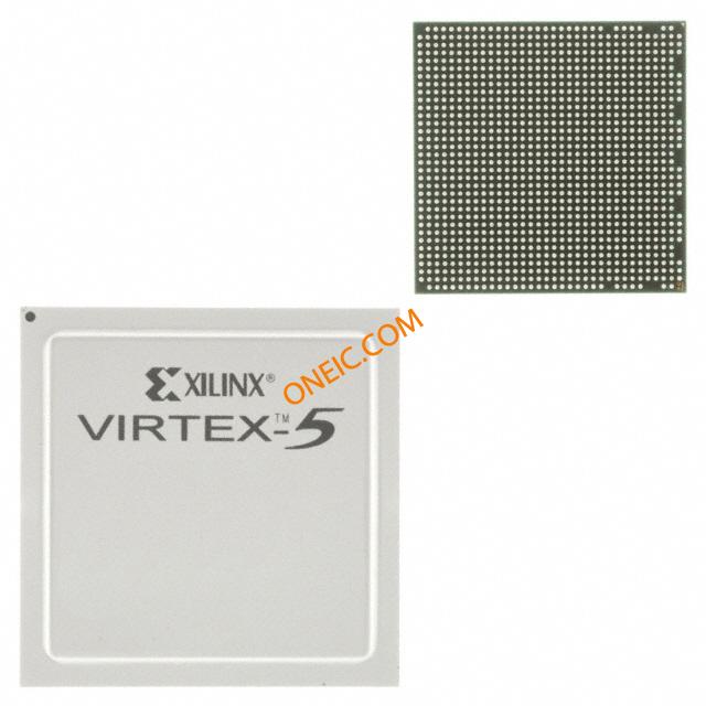
Xilinx- 1136-FBGA
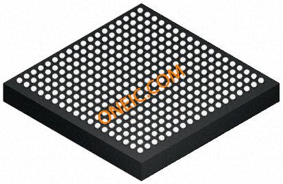
Image Preview
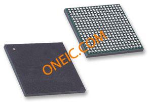
Image Preview