XC5VLX330T-1FF1738C
High-capacity FPGA chips for advanced electronic systems
Manufacturer: xilinx
series introduction
# Introduction to the XC5VLX330T - 1FF1738C Product Series
## 1. Overview
The XC5VLX330T - 1FF1738C belongs to the Virtex - 5 LX field - programmable gate array (FPGA) product series by Xilinx. FPGAs are integrated circuits that can be programmed and reprogrammed by the user after manufacturing, offering high flexibility and adaptability for a wide range of applications. This particular model is designed to meet the demanding requirements of high - performance and complex digital systems.
## 2. Key Features
### 2.1 Logic Resources
- **High - Density Logic**: The XC5VLX330T - 1FF1738C is equipped with a large number of configurable logic blocks (CLBs). These CLBs are the basic building blocks of the FPGA, allowing users to implement complex digital circuits such as arithmetic units, state machines, and data path elements. With a high logic density, it can handle large - scale designs, enabling the integration of multiple functions on a single chip.
- **Distributed and Block RAM**: It includes both distributed random - access memory (RAM) and block RAM. Distributed RAM is used for small - scale, high - speed storage requirements within the logic fabric, while block RAM provides larger - capacity memory blocks. This combination allows for efficient data storage and retrieval, which is crucial for applications such as digital signal processing (DSP) and data buffering.
### 2.2 DSP Resources
- **Embedded DSP Slices**: The FPGA features a significant number of embedded DSP slices. These slices are optimized for performing high - speed arithmetic operations, such as multiplication, addition, and accumulation. They are particularly useful in applications like digital filtering, image and video processing, and communication systems, where real - time signal processing is required.
- **High - Performance DSP Architecture**: The DSP slices in the XC5VLX330T - 1FF1738C are designed with a high - performance architecture that can operate at high clock frequencies. This enables the implementation of complex DSP algorithms with low latency and high throughput.
### 2.3 I/O and Connectivity
- **Multiple I/O Standards**: It supports a wide range of input/output (I/O) standards, including LVDS (Low - Voltage Differential Signaling), SSTL (Stub Series Terminated Logic), and HSTL (High - Speed Transceiver Logic). This flexibility allows the FPGA to interface with various external devices, such as memory chips, sensors, and communication interfaces.
- **High - Speed Transceivers**: The device is equipped with high - speed serial transceivers. These transceivers can operate at very high data rates, enabling high - bandwidth communication links. They are suitable for applications such as high - speed data transfer between boards, optical communication, and Ethernet interfaces.
### 2.4 Power Management
- **Low - Power Design**: Xilinx has implemented advanced power - management techniques in the XC5VLX330T - 1FF1738C. It offers multiple power - saving modes, allowing users to optimize the power consumption of the FPGA according to the application requirements. This is particularly important for battery - powered devices or systems where power efficiency is a critical factor.
- **Dynamic Power Management**: The FPGA can dynamically adjust its power consumption based on the workload. For example, during periods of low activity, it can enter a low - power state, reducing the overall power consumption without sacrificing performance when the workload increases.
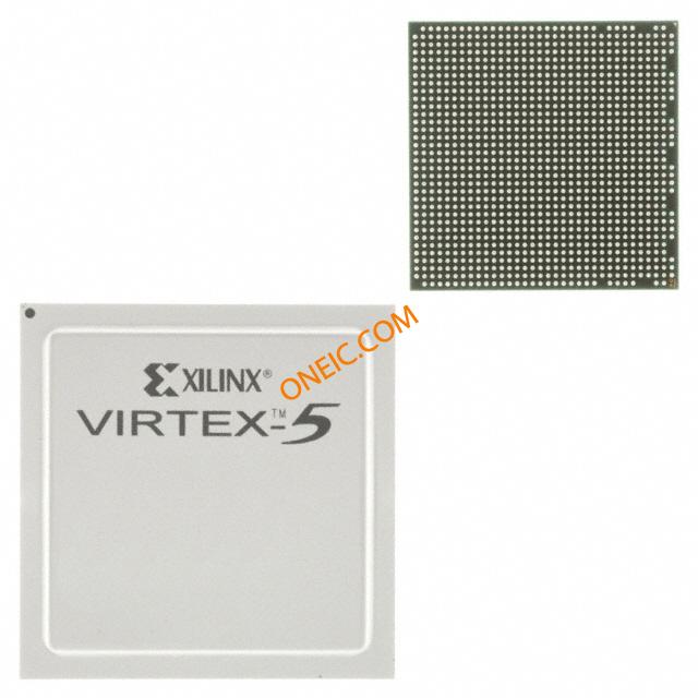
## 3. Package and Pinout
The "FF1738" in the product name refers to the package type. The fine - pitch ball grid array (FBGA) package with 1738
Images for reference
Xilinx- 1136-FBGA