XC3S250E-4VQG100I
Spartan-3E family FPGAs with 250K gates, 5508 cells, and 100-pin VTQFP package
Manufacturer: xilinx
series introduction
# Introduction to the XC3S250E - 4VQG100I Product Series
## 1. Overview
The XC3S250E - 4VQG100I belongs to the Spartan - 3E family of Field - Programmable Gate Arrays (FPGAs) developed by Xilinx. FPGAs are integrated circuits that can be programmed and reprogrammed by the user after manufacturing, offering a high degree of flexibility for a wide range of applications. This particular product in the series is designed to provide a cost - effective solution with a good balance of performance, functionality, and power consumption.
## 2. Key Features
### 2.1 Logic Resources
- **Slice Count**: The XC3S250E - 4VQG100I offers a significant number of logic slices. These slices are the basic building blocks of the FPGA, containing look - up tables (LUTs), flip - flops, and carry logic. With a sufficient number of slices, it can implement complex digital circuits, such as state machines, arithmetic units, and data path elements.
- **Configurable Logic Blocks (CLBs)**: Composed of multiple slices, CLBs provide a higher - level of logic organization. They allow for efficient implementation of larger digital functions by grouping related logic elements together.
### 2.2 Memory
- **Block RAM**: It is equipped with on - chip block RAM. Block RAMs are large, fast memory blocks that can be used for various purposes, such as storing data buffers, implementing FIFOs (First - In - First - Out), or as a small - scale memory for algorithms. The block RAMs can be configured in different sizes and data widths to meet the specific requirements of the application.
- **Distributed RAM**: In addition to block RAM, the FPGA also has distributed RAM, which is formed by the LUTs in the slices. Distributed RAM is useful for small - scale memory requirements and can be easily integrated into the logic design.
### 2.3 I/O Resources
- **I/O Pins**: The VQG100 package of the XC3S250E - 4VQG100I provides a specific number of I/O pins. These pins can be configured to support a variety of I/O standards, such as LVCMOS (Low - Voltage Complementary Metal - Oxide - Semiconductor), LVTTL (Low - Voltage Transistor - Transistor Logic), and others. This allows the FPGA to interface with different types of external devices, including microcontrollers, sensors, and communication modules.
- **I/O Banks**: The I/O pins are organized into banks, each of which can be independently configured for different voltage levels and I/O standards. This flexibility enables the FPGA to communicate with multiple external devices operating at different voltage levels simultaneously.
### 2.4 Speed Grade
The “- 4” in the part number indicates the speed grade of the FPGA. A higher speed grade generally means that the FPGA can operate at higher clock frequencies and has shorter propagation delays. This is crucial for applications that require high - speed data processing, such as high - speed communication interfaces and real - time signal processing.
### 2.5 Power Consumption
The XC3S250E - 4VQG100I is designed to be power - efficient. It uses advanced semiconductor manufacturing processes and power management techniques to minimize power consumption. This is especially important for battery - powered applications or systems where power dissipation is a concern, as it helps to reduce operating costs and extend the battery life.
## 3. Applications
### 3.1 Industrial Automation
- **Control Systems**: In industrial control systems, the FPGA can be used to implement complex control algorithms, such as PID (Proport
Images for reference
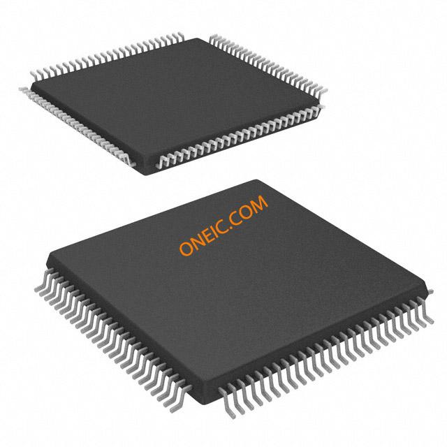
100TQFP
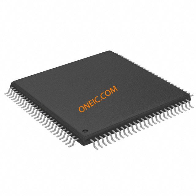
100-TQFP
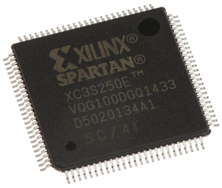
Image Preview