XC3S100E-4TQG144I
Compact Spartan-3E FPGAs with 100K gates for versatile digital applications
Manufacturer: xilinx
series introduction
# Introduction to the XC3S100E - 4TQG144I Product Series
## 1. Overview
The XC3S100E - 4TQG144I belongs to the Spartan - 3E family of Field - Programmable Gate Arrays (FPGAs) developed by Xilinx. FPGAs are integrated circuits that can be programmed and reprogrammed by the user after manufacturing, offering a high degree of flexibility for a wide range of applications. This particular product in the series is designed to provide cost - effective and high - performance solutions for various industries, including consumer electronics, industrial automation, and communication systems.
## 2. Key Features
### 2.1 Logic Resources
- **Logic Cells**: The XC3S100E - 4TQG144I is equipped with a sufficient number of logic cells. These logic cells are the building blocks of the FPGA, allowing users to implement complex digital circuits such as arithmetic units, state machines, and data processing modules. The logic cell architecture enables efficient implementation of combinational and sequential logic, providing the flexibility to design custom - tailored solutions.
- **Look - Up Tables (LUTs)**: LUTs are an essential part of the FPGA's logic fabric. They can be configured to implement any Boolean function of a given number of inputs. The XC3S100E - 4TQG144I has a specific number of LUTs that contribute to its overall logic capacity, enabling the implementation of complex algorithms and functions.
### 2.2 Memory Resources
- **Block RAM**: It includes Block RAM modules, which are large - scale memory blocks within the FPGA. These Block RAMs can be used for various purposes, such as data buffering, FIFO (First - In - First - Out) implementation, and storing configuration data. The ability to access and manipulate data in these memory blocks quickly is crucial for applications that require high - speed data processing.
- **Distributed RAM**: In addition to Block RAM, the device also has distributed RAM. Distributed RAM is smaller in size but more widely distributed across the FPGA fabric. It can be used for storing small amounts of data close to the logic that needs to access it, reducing the data access latency.
### 2.3 I/O Resources
- **I/O Pins**: The XC3S100E - 4TQG144I comes with a set of I/O pins. These pins can be configured to support different I/O standards, such as LVCMOS (Low - Voltage Complementary Metal - Oxide - Semiconductor), LVTTL (Low - Voltage Transistor - Transistor Logic), and others. This flexibility allows the FPGA to interface with a wide variety of external devices, including microcontrollers, sensors, and communication modules.
- **I/O Banks**: The I/O pins are organized into I/O banks, which can be independently powered and configured. This feature provides isolation and flexibility in power management and I/O standard selection, making it easier to interface with different voltage domains.
### 2.4 Speed Grade
The “- 4” in the part number indicates the speed grade of the XC3S100E - 4TQG144I. A higher speed grade generally means that the FPGA can operate at higher clock frequencies, resulting in faster data processing and shorter propagation delays. This is particularly important for applications that require high - speed data transfer and real - time processing, such as high - speed communication interfaces and video processing.
### 2.5 Package Type
The “TQG144” represents the package type of the device. It is a 144 - pin Thin Quad Flat Pack (TQFP). This package offers a relatively small form factor, making
Images for reference

144-LQFP
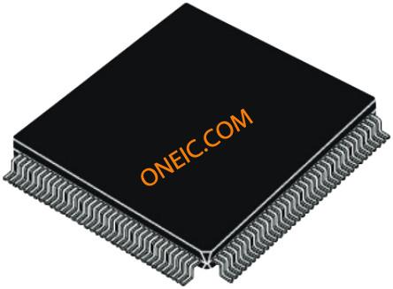
Image Preview
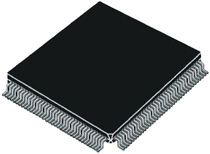
Image Preview