UA741CDT
General-purpose single operational amplifiers in 8-pin SOIC format
Manufacturer: stm
series introduction
# Introduction to the UA741CDT Product Series
## 1. Overview
The UA741CDT is a well - known and widely used operational amplifier (op - amp) product series. Operational amplifiers are fundamental building blocks in analog electronics, and the UA741CDT offers a reliable and cost - effective solution for a vast array of applications.
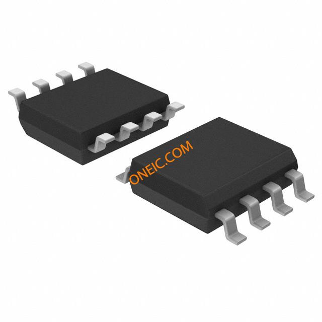
## 2. Package and Pin Configuration
### Package
The "CDT" in the UA741CDT indicates the package type. It typically comes in a small - outline integrated circuit (SOIC) package. This surface - mount package is popular in modern printed circuit board (PCB) designs due to its compact size, which allows for high - density component placement. The SOIC package also provides good mechanical stability and electrical performance, making it suitable for automated assembly processes.
### Pin Configuration
The UA741CDT has a standard 8 - pin configuration.
- **Pin 1 and Pin 5**: These are the offset null pins. They are used to adjust the output offset voltage of the op - amp to zero when the input voltages are equal. By connecting a potentiometer between these two pins and the negative power supply, fine - tuning of the offset can be achieved.
- **Pin 2**: This is the inverting input terminal. A signal applied to this pin will result in an inverted output at the op - amp's output terminal.
- **Pin 3**: The non - inverting input terminal. Signals applied here will produce a non - inverted output at the output terminal.
- **Pin 4**: The negative power supply pin. It is connected to the negative voltage source, which is typically a negative DC voltage in a dual - power - supply configuration.
- **Pin 6**: The output terminal. The amplified signal is available at this pin.
- **Pin 7**: The positive power supply pin. It is connected to the positive voltage source, usually a positive DC voltage in a dual - power - supply setup.
- **Pin 8**: This pin is typically left unconnected in most applications.
## 3. Electrical Characteristics
### Input Characteristics
- **Input Offset Voltage**: The UA741CDT has a relatively low input offset voltage, typically in the range of a few millivolts. This parameter represents the voltage difference that must be applied between the inverting and non - inverting inputs to make the output voltage zero. A low input offset voltage is crucial for applications where high - precision amplification is required.
- **Input Bias Current**: The input bias current is the average of the currents flowing into the inverting and non - inverting input terminals. In the UA741CDT, the input bias current is in the order of nanoamperes. Low input bias current helps to minimize errors in circuits where the source impedance is high.
- **Input Resistance**: The input resistance of the UA741CDT is very high, typically in the order of megohms. This high input resistance ensures that the op - amp draws very little current from the input source, thus minimizing the loading effect on the preceding circuit.
### Output Characteristics
- **Output Voltage Swing**: The op - amp can swing its output voltage over a wide range, typically close to the power supply voltages. For example, in a ±15V power - supply configuration, the output voltage can swing from approximately - 13V to + 13V.
- **Output Current**: The UA741CDT can supply a certain amount of output current. It can typically source or sink a few milliamperes of current, which is sufficient for driving many types of loads such as small - signal transistors, resistive loads, and some types of sensors.
### Gain and Bandwidth
- **Open
Images for reference
8-SOIC

Image Preview

Image Preview