TPS560200DBV
Compact synchronous step-down voltage regulators for efficient power conversion
Manufacturer: ti
series introduction
# TPS560200DBV Product Series Introduction
## 1. Overview
The TPS560200DBV is a remarkable product series within the realm of power management integrated circuits (PMICs) developed by Texas Instruments. This series is specifically engineered to meet the diverse and demanding power requirements of modern electronic devices, offering a high - performance, efficient, and reliable solution for a wide range of applications.
## 2. Key Features
### 2.1 High Efficiency
One of the standout features of the TPS560200DBV series is its high efficiency. It utilizes advanced power conversion topologies and low - resistance internal components. This results in minimal power loss during the conversion process, which is crucial for battery - powered devices as it helps to extend battery life. For example, in portable consumer electronics such as smartphones and tablets, the high efficiency of the TPS560200DBV can significantly reduce the amount of power wasted as heat, allowing the device to operate for longer periods on a single charge.
### 2.2 Wide Input Voltage Range
The series supports a wide input voltage range. This flexibility enables it to be used in various power supply scenarios. Whether the input power source is a low - voltage battery or a higher - voltage power adapter, the TPS560200DBV can handle it. For instance, it can accept input voltages from a few volts up to a relatively high value, making it suitable for applications that may experience fluctuations in the input power, such as automotive electronics where the battery voltage can vary depending on the vehicle's operating conditions.
### 2.3 Adjustable Output Voltage
The output voltage of the TPS560200DBV is adjustable. Designers can easily configure the output voltage according to the specific requirements of the load. This is extremely useful in applications where different components within a system may require different supply voltages. For example, in a complex printed circuit board (PCB) with multiple integrated circuits, some components may need a 1.8V supply, while others may require 3.3V. The adjustable output voltage feature of the TPS560200DBV allows for a single power management solution to meet these diverse needs.
### 2.4 Low Quiescent Current
The series has a low quiescent current, which is the current consumed by the device when it is in a standby or light - load condition. This is an important feature for applications that spend a significant amount of time in standby mode, such as IoT devices. A low quiescent current ensures that the device does not draw excessive power when it is not actively performing its main function, thereby conserving energy and reducing overall power consumption.
### 2.5 Over - Current and Over - Temperature Protection
To ensure the reliability and safety of the system, the TPS560200DBV is equipped with over - current and over - temperature protection mechanisms. In the event of an over - current situation, such as a short - circuit in the load, the device will automatically limit the current to prevent damage to itself and the connected components. Similarly, if the temperature of the device rises above a certain threshold due to excessive power dissipation, the over - temperature protection will kick in, either by reducing the output power or shutting down the device temporarily until the temperature returns to a safe level.
## 3. Package and Pin Configuration
The TPS560200DBV comes in a specific package that offers several advantages. The package is designed to provide good thermal performance, allowing the device to dissipate heat effectively. It also has a compact form factor, which is beneficial for space - constrained applications. The pin configuration of the device is well - thought - out, with clearly defined pins for input voltage, output voltage, ground
Images for reference
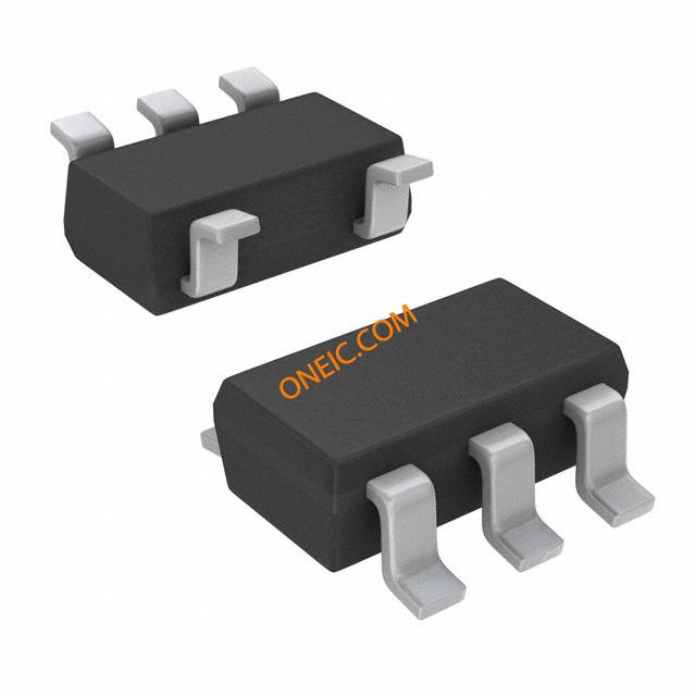
SOT-23-5, SC-74A
Image Preview
Image Preview