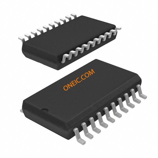
TPIC6B595DW
8-bit shift register ICs for serial to parallel data conversion
Manufacturer: ti
series introduction
# TPIC6B595DW Product Series Introduction
## 1. Overview
The TPIC6B595DW is a highly versatile and efficient integrated circuit product series that belongs to the shift register family. It is specifically designed to provide a cost - effective and space - saving solution for expanding the output capabilities of microcontrollers and other digital control systems. This product series is widely used in various applications, including industrial automation, consumer electronics, automotive electronics, and display systems.
## 2. Key Features
### 2.1 High - Current Sink Capability
One of the most prominent features of the TPIC6B595DW is its ability to sink high currents. Each output can sink up to 150 mA of continuous current, which makes it suitable for driving a wide range of loads such as LEDs, relays, and small motors. This high - current handling capacity eliminates the need for external power - boosting components in many applications, simplifying the circuit design and reducing costs.
### 2.2 Serial Input/Parallel Output Operation
The TPIC6B595DW operates in a serial - in, parallel - out mode. It allows data to be shifted in serially using a single data input line (DS), a clock input line (SHCP), and a latch enable line (STCP). Once the data is shifted in, it can be latched and presented at the parallel outputs simultaneously. This feature is extremely useful when dealing with limited I/O pins on a microcontroller, as it enables the expansion of output channels with just a few control lines.
### 2.3 8 - Bit Shift Register and Output Latch
The device contains an 8 - bit shift register and an output latch. The shift register stores the incoming serial data, and the output latch holds the data that is to be presented at the outputs. This separation of the shift register and the output latch allows for asynchronous data transfer and updating of the outputs. The output latch can be updated independently of the shift register, providing flexibility in controlling the timing of output changes.
### 2.4 Output Enable Control
The TPIC6B595DW has an output enable (OE) pin. When this pin is pulled low, the outputs are enabled, and the data stored in the output latch is presented at the outputs. When the OE pin is pulled high, the outputs are disabled, and they are set to a high - impedance state. This feature is useful for applications where the outputs need to be temporarily disabled, such as during power - on reset or when performing diagnostic tests.
### 2.5 Cascadeable Design
Multiple TPIC6B595DW devices can be cascaded together to increase the number of output channels. By connecting the serial output (Q7S) of one device to the serial input (DS) of the next device, it is possible to create a chain of shift registers. This allows for easy expansion of the output capabilities without the need for additional control lines from the microcontroller.
## 3. Electrical Characteristics
### 3.1 Supply Voltage
The TPIC6B595DW operates over a wide supply voltage range of 4.5V to 5.5V. This makes it compatible with most standard digital logic circuits and power supplies commonly used in electronic systems.
### 3.2 Input and Output Logic Levels
The input logic levels are compatible with TTL and CMOS logic families. The high - level input voltage (VIH) is typically 2V, and the low - level input voltage (VIL) is typically 0.8V. The output logic levels are also well - defined, with a low - level output voltage (VOL) of less than 1V when sinking the rated current.
### 3.3 Operating Temperature Range
The device is designed to
Images for reference

20-SOIC 0.295

20-SOIC 0.295

Image Preview