TLV62065DSG
Compact 2A step-down voltage regulators for DC-DC conversion
Manufacturer: ti
series introduction
# TLV62065DSG Product Series Introduction
## 1. Overview
The TLV62065DSG belongs to a highly efficient and versatile product series designed for power management applications. It is a step - down (buck) DC - DC converter integrated circuit that offers a compact and reliable solution for converting higher input voltages to lower, regulated output voltages. This series is well - suited for a wide range of electronic devices, from portable consumer electronics to industrial control systems.
## 2. Key Features
### High Efficiency
- The TLV62065DSG is engineered to achieve high conversion efficiency, which is crucial for battery - powered devices. By minimizing power losses during the voltage conversion process, it helps to extend the battery life of portable devices such as smartphones, tablets, and wearables. For example, in typical operating conditions, it can achieve efficiency levels of up to 95%, reducing the amount of wasted energy as heat.
### Wide Input Voltage Range
- It supports a wide input voltage range, typically from 2.3 V to 6 V. This flexibility allows it to be used with various power sources, including single - cell lithium - ion batteries (which typically have an output voltage range of around 3 - 4.2 V) and multi - cell alkaline battery packs. This wide input range makes it suitable for a diverse set of applications with different power supply requirements.
### Adjustable Output Voltage
- The output voltage of the TLV62065DSG can be easily adjusted using external resistors. This feature provides designers with the flexibility to customize the output voltage according to the specific needs of their application. The output voltage can be set within a certain range, typically from 0.6 V to the input voltage, enabling it to power a variety of components such as microcontrollers, sensors, and other low - voltage integrated circuits.
### Low Quiescent Current
- In standby or light - load conditions, the TLV62065DSG has a very low quiescent current. This means that it consumes minimal power when the load is small, further enhancing the overall power efficiency of the system. For battery - powered devices that spend a significant amount of time in standby mode, this low quiescent current feature is essential for conserving battery energy.
### Small Package Size
- The TLV62065DSG comes in a small and space - saving package, such as the DSG package. This compact form factor is ideal for applications where board space is limited, such as in small - form - factor portable devices and IoT (Internet of Things) sensors. The small package also helps to reduce the overall size and weight of the end - product.
## 3. Functional Block Diagram and Operation
### Block Diagram
- The TLV62065DSG consists of several key functional blocks, including an input voltage regulator, a power switch, an inductor, a capacitor, and a control circuit. The input voltage is first regulated to ensure stable operation. The power switch, controlled by the internal control circuit, switches on and off at a high frequency to transfer energy from the input to the output through the inductor. The capacitor at the output helps to filter the output voltage and reduce ripple.
### Operation
- When the power switch is turned on, current flows through the inductor, storing energy in its magnetic field. When the switch is turned off, the inductor releases the stored energy, maintaining the current flow to the output. The control circuit continuously monitors the output voltage and adjusts the duty cycle of the power switch to maintain a stable output voltage, even when the input voltage or load current changes.
## 4. Applications
### Portable Consumer Electronics
- In smartphones and tablets, the TLV62065DSG can be used to power various subs
Images for reference
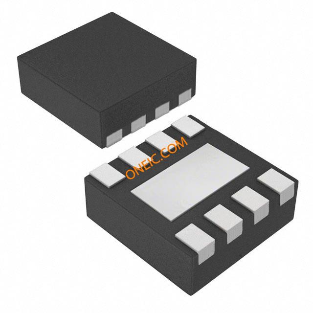
8-WFDFN Exposed Pad
Image Preview
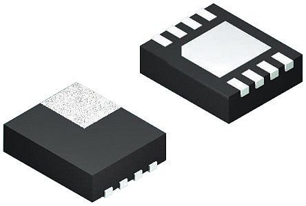
Image Preview