TLV2472QDRQ1
General-purpose automotive operational amplifiers with rail-to-rail input/output
Manufacturer: ti
series introduction
# TLV2472QDRQ1 Product Series Introduction
## 1. Overview
The TLV2472QDRQ1 is a high - performance operational amplifier (op - amp) product series specifically designed to meet the demanding requirements of automotive and other high - reliability applications. Texas Instruments, a leading semiconductor manufacturer, has engineered this series to offer a combination of excellent electrical characteristics, robustness, and compliance with automotive standards.
## 2. Key Features
### 2.1 Low Power Consumption
One of the standout features of the TLV2472QDRQ1 is its low power consumption. In today's automotive and portable electronics applications, power efficiency is crucial. This op - amp series operates on a low supply current, which helps in extending the battery life of portable devices and reducing the overall power consumption in automotive systems. This is especially important in applications where power is limited, such as in sensor nodes and battery - powered automotive accessories.
### 2.2 Rail - to - Rail Input and Output
The TLV2472QDRQ1 offers rail - to - rail input and output capabilities. This means that the input voltage range can extend from the negative supply rail to the positive supply rail, and the output voltage can swing very close to both supply rails. This feature is highly beneficial in applications where the full range of the supply voltage needs to be utilized, such as in signal conditioning circuits for sensors that produce low - level signals close to the supply rails.
### 2.3 High Gain Bandwidth Product
It has a relatively high gain - bandwidth product. This parameter determines the frequency range over which the op - amp can amplify signals with a specified gain. A high gain - bandwidth product allows the TLV2472QDRQ1 to be used in applications that require amplification of high - frequency signals, such as in communication systems and high - speed data acquisition circuits.
### 2.4 Low Input Offset Voltage
The low input offset voltage of the TLV2472QDRQ1 ensures accurate signal amplification. Input offset voltage is the voltage that must be applied between the input terminals to make the output voltage zero. A low offset voltage reduces the error in the amplified signal, making it suitable for precision measurement applications, such as in automotive sensor interfaces where accurate signal processing is essential.
### 2.5 Automotive - Grade Qualification
The TLV2472QDRQ1 is AEC - Q100 qualified, which is a set of stress test qualification requirements for automotive - grade integrated circuits. This qualification ensures that the product can withstand the harsh environmental conditions typically encountered in automotive applications, including temperature variations, vibration, and electrical noise. It provides high reliability and long - term stability, making it a trusted choice for automotive designers.
## 3. Package and Pinout
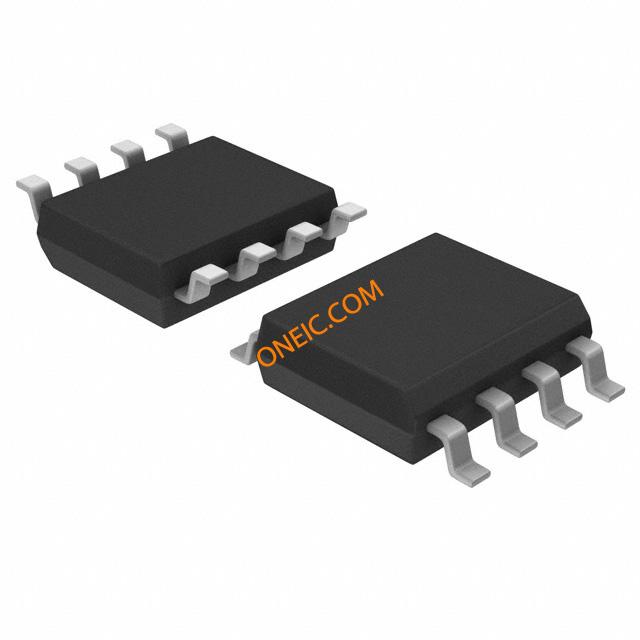
The TLV2472QDRQ1 is available in a small - outline integrated circuit (SOIC) package, which is a popular choice for surface - mount applications. The package offers good thermal performance and is easy to assemble on printed circuit boards (PCBs). The pinout of the TLV2472QDRQ1 is designed in a standard configuration, with clearly defined input, output, and power supply pins. This makes it easy for designers to integrate the op - amp into their circuits without having to deal with complex pin arrangements.
## 4. Applications
### 4.1 Automotive Sensor Interfaces
In automotive applications, sensors are used to measure various parameters such as temperature, pressure, and position. The TLV2472QDRQ1 can be used as a signal conditioner for these sensors. Its low power consumption, low input offset voltage, and rail - to - rail capabilities make it ideal for amplifying and conditioning the low - level signals produced by sensors, ensuring accurate measurement
Images for reference

8-SOIC

8-SOIC

Image Preview