TLC542IN
8-bit analog-to-digital converters with SPI interface, 20-pin PDIP packaging
Manufacturer: ['rochester', 'analog-devices', 'ti']
series introduction
# Introduction to the TLC542IN Product Series
## Overview
The TLC542IN is a highly regarded and widely used product series within the realm of analog - to - digital converters (ADCs). Texas Instruments, a global leader in semiconductor technology, manufactures this series. These ADCs play a crucial role in modern electronic systems by converting analog signals, which are continuous in nature, into digital signals that can be processed, stored, and analyzed by digital circuits and microprocessors.
## Key Features
### High - Speed Conversion
One of the standout features of the TLC542IN series is its relatively high - speed conversion capability. It can perform analog - to - digital conversions at a rate that makes it suitable for a variety of real - time applications. This speed allows the device to quickly capture and convert analog input signals, ensuring that the digital representation closely follows the changes in the analog signal. For example, in audio processing applications, where the audio signal is constantly changing, the high - speed conversion of the TLC542IN enables accurate digitization of the sound waves, preserving the quality of the audio.
### 8 - Bit Resolution
The TLC542IN offers 8 - bit resolution. This means that it can divide the input analog voltage range into 2^8 (256) discrete levels. The 8 - bit resolution provides a good balance between accuracy and cost - effectiveness. In many applications where a moderate level of precision is required, such as simple sensor interfaces or basic control systems, the 8 - bit resolution of the TLC542IN is sufficient. It allows for a reasonable level of detail in representing the analog input signal in the digital domain.
### Serial Interface
The series is equipped with a serial interface. This type of interface simplifies the connection between the ADC and other digital components in a system, such as microcontrollers or digital signal processors. Serial interfaces require fewer pins compared to parallel interfaces, which reduces the complexity of the printed circuit board (PCB) layout and saves valuable board space. Additionally, the serial communication protocol used by the TLC542IN is well - defined and easy to implement, making it accessible for designers with different levels of experience.
### Low Power Consumption
Power efficiency is a critical factor in many electronic applications, especially those that rely on battery power or have strict power budget constraints. The TLC542IN series is designed with low power consumption in mind. It operates at relatively low supply voltages and consumes minimal current during both conversion and standby modes. This makes it an ideal choice for portable devices, wireless sensor nodes, and other battery - powered applications where long battery life is essential.
## Functional Block Diagram and Working Principle
### Input Stage
The input stage of the TLC542IN is designed to accept analog input signals. It has a specified input voltage range within which it can accurately convert the analog signal. The input impedance of the device is carefully designed to minimize the loading effect on the source of the analog signal. This ensures that the ADC does not significantly alter the characteristics of the input signal, allowing for accurate conversion.
### Conversion Core
The conversion core is the heart of the TLC542IN. It uses a successive - approximation algorithm to perform the analog - to - digital conversion. In this algorithm, the ADC compares the input analog voltage with a series of reference voltages generated internally. Based on the comparison results, it determines the digital code that represents the input voltage. The successive - approximation process is repeated until the digital code accurately represents the input analog voltage within the specified resolution.
### Output Stage
The output stage of the TLC542IN is responsible for transmitting the digital conversion result to the external digital components. Through the serial interface, the 8 - bit digital code is sent out in a sequential manner. The output data is formatted according to the communication protocol of the serial interface, making it easy for
Images for reference
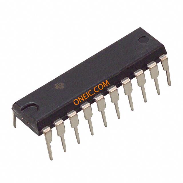
20-DIP,R-PDIP-Txx
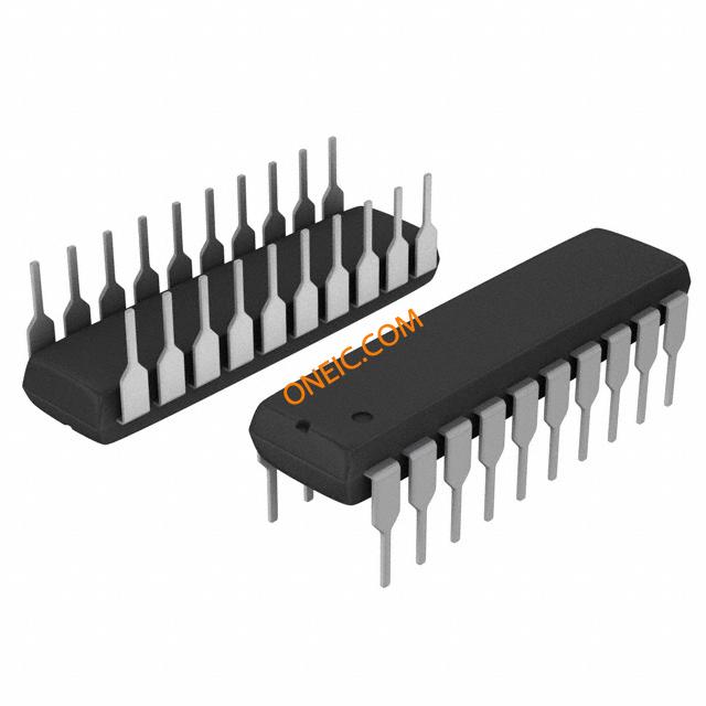
20-DIP
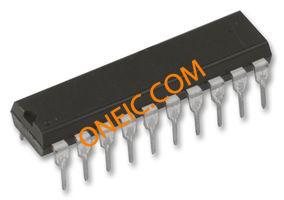
Image Preview