SN74S280NE4
9-bit parity generator/checker IC in 14-pin DIP format
Manufacturer: ti
series introduction
# Introduction to the SN74S280NE4 Product Series
## 1. Overview
The SN74S280NE4 belongs to the 74S series of integrated circuits, which are well - known for their high - speed operation and reliability in digital logic applications. This specific product is a 9 - bit odd/even parity generator/checker, designed to perform crucial functions in data communication and error - detection systems.
## 2. Key Features
### 2.1 High - Speed Performance
One of the standout features of the SN74S280NE4 is its high - speed operation. The Schottky TTL (Transistor - Transistor Logic) technology used in its design allows for fast switching times. This makes it suitable for applications where data needs to be processed quickly, such as in high - speed data transmission lines, computer buses, and real - time digital systems.
### 2.2 Parity Generation and Checking
The primary function of the SN74S280NE4 is to generate and check parity. Parity is a simple form of error - detection in digital data. It can determine whether the number of logic high (1) bits in a given data set is odd or even. In a 9 - bit system, the device can generate a parity bit based on the input data bits, which can then be transmitted along with the data. At the receiving end, the same device can be used to check the parity of the received data, including the transmitted parity bit. If the parity does not match the expected value, it indicates that an error has likely occurred during transmission.
### 2.3 Wide Operating Voltage Range
The SN74S280NE4 can operate within a relatively wide voltage range. This flexibility allows it to be integrated into various electronic systems with different power supply requirements. It typically operates with a supply voltage (VCC) in the range of 4.75V to 5.25V, which is common in many digital circuits.
### 2.4 Compatibility
It is compatible with other TTL - based integrated circuits. This means that it can be easily interfaced with other components in a digital system, such as microprocessors, memory chips, and other logic gates. This compatibility simplifies the design process and reduces the need for additional level - shifting circuits.
## 3. Pin Configuration
The SN74S280NE4 comes in a standard 16 - pin dual - in - line package (DIP). Here is a brief description of the key pins:
### 3.1 Input Pins
- **A - I**: These are the 9 input pins where the data bits are applied. The device analyzes the logic levels on these pins to perform parity generation or checking.
### 3.2 Output Pins
- **YODD**: This pin provides the odd - parity output. If the number of high - level inputs among the 9 data inputs is odd, the YODD pin will be at a high logic level.
- **YEVEN**: This pin gives the even - parity output. When the number of high - level inputs among the 9 data inputs is even, the YEVEN pin will be at a high logic level.
### 3.3 Power and Ground Pins
- **VCC**: This is the positive power supply pin, which should be connected to a stable 5V power source within the specified voltage range.
- **GND**: The ground pin, which provides the reference voltage for the circuit.
## 4. Applications
### 4.1 Data Communication
In serial and parallel data communication systems, the SN74S280NE4 can be used to add parity bits to the data before transmission. At the receiving
Images for reference
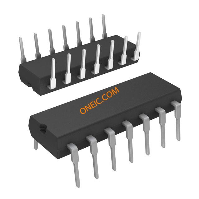
14-DIP