SN74LVTH541NSR
3.3V octal buffers and drivers with 3-state outputs for signal management
Manufacturer: ['rochester', 'analog-devices', 'ti']
series introduction
# SN74LVTH541NSR Product Series Introduction
## 1. Overview
The SN74LVTH541NSR is a member of the Texas Instruments' logic family, specifically designed to meet the requirements of modern digital systems. This octal buffer/line driver with 3 - state outputs offers high - performance and reliable signal buffering and driving capabilities, making it an ideal choice for a wide range of applications in the electronics industry.
## 2. Key Features
### 2.1. Voltage Compatibility
- **Low - Voltage Operation**: The SN74LVTH541NSR is designed to operate with a supply voltage range of 2.7V to 3.6V. This low - voltage operation makes it suitable for use in battery - powered devices and modern low - power digital systems, helping to reduce power consumption and extend battery life.
- **Voltage - Level Translation**: It can interface between different voltage domains. For example, it can translate signals from a 3.3V system to a compatible logic level, enabling seamless communication between components operating at different voltage levels.
### 2.2. High - Speed Performance
- **Fast Propagation Delay**: With a typical propagation delay in the range of a few nanoseconds, the SN74LVTH541NSR can handle high - speed data transfer. This makes it well - suited for applications where rapid signal processing and data transmission are required, such as in high - speed data buses and communication interfaces.
- **High - Frequency Operation**: It can operate at relatively high frequencies, allowing it to keep up with the fast - paced data rates of modern digital systems.
### 2.3. 3 - State Outputs
- **Output Enable Control**: The device features 3 - state outputs, which can be controlled using an output enable (OE) pin. When the OE pin is active, the outputs are enabled, and the device functions as a normal buffer/line driver. When the OE pin is inactive, the outputs are placed in a high - impedance state, effectively disconnecting the device from the output bus. This feature is crucial for bus - sharing applications, where multiple devices need to share a common data bus without interfering with each other.
### 2.4. ESD Protection
- **Robust Electrostatic Discharge (ESD) Protection**: The SN74LVTH541NSR is equipped with ESD protection on all inputs and outputs. This protection helps to safeguard the device from damage caused by electrostatic discharge events, which are common in electronic environments. It enhances the reliability and durability of the device, reducing the risk of failure due to ESD - induced damage.
## 3. Functional Description
### 3.1. Buffer/Line Driver Function
The SN74LVTH541NSR consists of eight independent buffer/line driver circuits. Each input is connected to a corresponding output through a buffer stage. The buffer amplifies the input signal and provides a high - drive - capability output, which can be used to drive long traces on a printed circuit board (PCB) or to interface with other components that require a stronger signal.
### 3.2. Output Enable Logic
The output enable (OE) pin is used to control the state of the outputs. The OE pin is active - low, meaning that when the OE pin is pulled low (logic 0), the outputs are enabled, and the input signals are passed through to the outputs. When the OE pin is pulled high (logic 1), the outputs are placed in a high - impedance state, and the device does not drive the output bus.
## 4. Applications
### 4.1. Data Bus Interfacing
- In computer systems and microcontroller - based applications, the SN
Images for reference
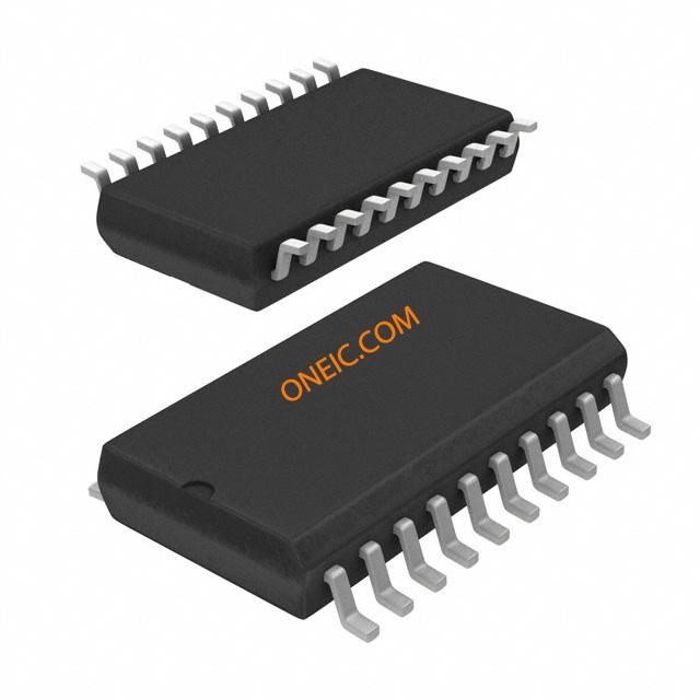
20-SOIC
Image Preview
Image Preview