SN74LVTH16373DGGR
16-bit transparent D-type latches with tri-state outputs in TSSOP packaging
Manufacturer: ['rochester', 'ti']
series introduction
# SN74LVTH16373DGGR Product Series Introduction
## 1. Overview
The SN74LVTH16373DGGR belongs to the SN74LVTH series of integrated circuits, which are designed to meet the requirements of modern digital systems. This particular device is a 16 - bit transparent D - type latch with 3 - state outputs. It is manufactured by Texas Instruments, a leading semiconductor company known for its high - quality and reliable electronic components.
## 2. Key Features
### 2.1 Bit - Width and Functionality
- **16 - Bit Operation**: With 16 bits of data handling capacity, the SN74LVTH16373DGGR can manage large amounts of digital information simultaneously. This makes it suitable for applications where wide - bus data transfer is required, such as in memory interfaces, data acquisition systems, and high - speed communication devices.
- **Transparent D - Type Latch**: The transparent latch operation means that the output follows the input when the latch enable (LE) input is high. When the LE input goes low, the data present at the input is latched, and the output retains that value until the LE is activated again. This feature is useful for temporarily storing data in a digital system.
### 2.2 3 - State Outputs
- The 3 - state outputs provide an additional level of flexibility. In the high - impedance (Hi - Z) state, the outputs are effectively disconnected from the circuit. This allows multiple devices to share a common bus without interfering with each other. For example, in a multi - master system, different devices can be enabled or disabled on the bus using the 3 - state control, preventing data conflicts.
### 2.3 Low - Voltage Operation
- The SN74LVTH16373DGGR is designed to operate at low voltages, typically in the range of 2.7V to 3.6V. This low - voltage operation offers several advantages, including reduced power consumption, which is crucial for battery - powered devices such as portable electronics, laptops, and handheld measurement instruments. It also helps in minimizing heat generation, improving the overall reliability of the system.
### 2.4 High - Speed Performance
- It can handle high - speed data transfer rates, making it suitable for applications that require fast data processing. The device has a short propagation delay, which ensures that the output responds quickly to changes in the input. This high - speed performance is essential in applications like high - speed data communication interfaces, where real - time data transfer is necessary.
## 3. Pin Configuration and Package
### 3.1 Pin Configuration
- The SN74LVTH16373DGGR has a well - defined pinout. It includes 16 data input pins (D0 - D15), 16 data output pins (Q0 - Q15), two latch enable pins (LE1 and LE2), two output enable pins (OE1# and OE2#), and power supply pins (VCC and GND). The separate latch enable and output enable pins allow for independent control of the latching and output states, providing greater flexibility in system design.
### 3.2 Package
- It comes in a TSSOP (Thin Shrink Small Outline Package) package. The TSSOP package is a surface - mount package that offers a compact form factor, which is beneficial for space - constrained applications. It also provides good thermal performance and ease of assembly on printed circuit boards (PCBs).
## 4. Electrical Characteristics
### 4.1 Input and Output Voltage Levels
- The input voltage levels are compatible with standard TTL (Transistor - Transistor Logic) and CMOS (Complementary Metal - Oxide
Images for reference

48-TSSOP
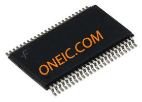
Image Preview
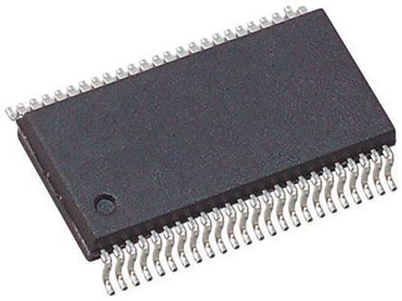
Image Preview