SN74LVT16244BZRDR
3.3V 16-bit buffers and drivers with 3-state outputs
Manufacturer: ['rochester', 'analog-devices', 'ti']
series introduction
# Introduction to the SN74LVT16244BZRDR Product Series
## 1. Overview
The SN74LVT16244BZRDR belongs to the SN74LVT family of integrated circuits, which are designed to meet the requirements of modern digital systems. This particular product is a 16 - bit buffer/driver with 3 - state outputs, offering high - performance and reliable signal buffering and driving capabilities. It is widely used in various applications where signal isolation, level shifting, and high - speed data transfer are crucial.
## 2. Key Features
### 2.1 High - Speed Operation
- The SN74LVT16244BZRDR is capable of operating at high clock frequencies, making it suitable for high - speed digital systems. It can handle fast - changing input signals and provide quick output responses, which is essential for applications such as data communication, microprocessor interfaces, and high - speed memory systems.
- With its low propagation delay, the device ensures that the output signals closely follow the input signals in a timely manner, minimizing the risk of data errors due to signal delays.
### 2.2 3 - State Outputs
- One of the significant features of this product is its 3 - state outputs. The 3 - state control allows the outputs to be in a high - impedance state, effectively disconnecting the device from the output bus. This feature is extremely useful in bus - oriented systems where multiple devices share the same bus. By enabling or disabling the 3 - state outputs, the SN74LVT16244BZRDR can be easily integrated into a multi - device system without causing bus contention.
### 2.3 Wide Supply Voltage Range
- It supports a wide supply voltage range, typically from 2.7V to 3.6V. This flexibility in power supply allows the device to be used in different power - management scenarios and makes it compatible with a variety of digital systems that operate at different voltage levels. It also provides some tolerance to power supply fluctuations, enhancing the overall reliability of the system.
### 2.4 Low Power Consumption
- The SN74LVT16244BZRDR is designed with low - power consumption in mind. This is achieved through advanced semiconductor manufacturing processes and circuit design techniques. Low power consumption not only reduces the overall power requirements of the system but also helps in minimizing heat generation, which is beneficial for the long - term stability and reliability of the device and the entire system.
### 2.5 ESD Protection
- The device is equipped with electrostatic discharge (ESD) protection on all inputs and outputs. ESD protection is crucial as it safeguards the integrated circuit from damage caused by static electricity, which can occur during handling, installation, or normal operation. This protection feature enhances the durability and reliability of the SN74LVT16244BZRDR, reducing the risk of premature failure due to ESD events.
## 3. Functional Description
### 3.1 Input and Output Configuration
- The SN74LVT16244BZRDR has 16 input pins and 16 output pins, arranged in a specific pin - out configuration. The inputs are designed to accept standard TTL or CMOS logic levels, making it compatible with a wide range of digital signal sources. The outputs are capable of driving capacitive loads, providing sufficient current to ensure proper signal transmission over the output lines.
- The device is divided into two independent 8 - bit sections, each with its own 3 - state control input. This allows for independent control of the two 8 - bit groups, providing greater flexibility in system design.
### 3.2 Logic Operation
- When the 3 - state control input (OE
Images for reference

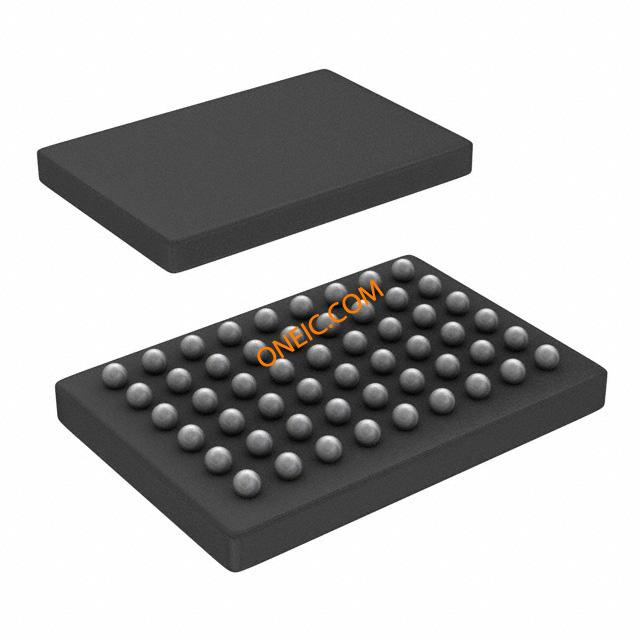
54-BGA-Micro-Jr-GRD

Image Preview