SN74LVC8T245DBR
8-bit bus transceiver with voltage translation in 24-pin SSOP package
Manufacturer: ti
series introduction
# SN74LVC8T245DBR Product Series Introduction
## 1. Overview
The SN74LVC8T245DBR is a member of Texas Instruments' extensive line of logic and interface products. This particular device belongs to the transceiver family, designed to provide bidirectional voltage-level translation and signal buffering capabilities. It is engineered to meet the requirements of modern electronic systems, offering high - speed performance, low power consumption, and compatibility with a wide range of voltage levels.
## 2. Key Features
### 2.1 Voltage - Level Translation
- **Wide Voltage Range**: The SN74LVC8T245DBR supports voltage translation between two different voltage domains. It can operate with supply voltages (VCC) ranging from 1.65V to 3.6V on both the A and B ports. This flexibility allows it to interface between different logic families, such as 1.8V, 2.5V, and 3.3V systems, enabling seamless communication between components operating at different voltage levels.
- **Bi - directional Translation**: It can perform bidirectional voltage - level conversion, meaning that data can flow in either direction between the A and B ports. This is crucial in applications where data needs to be transferred back and forth between different parts of a system with different voltage requirements.
### 2.2 High - Speed Performance
- **Fast Propagation Delay**: The device features a low propagation delay, which is essential for high - speed data transfer applications. With a typical propagation delay in the range of a few nanoseconds, it can handle high - frequency signals without significant signal degradation, ensuring that data is transmitted accurately and in a timely manner.
- **High - Speed Data Rates**: It is capable of supporting high - speed data rates, making it suitable for use in applications such as high - speed serial interfaces, memory interfaces, and data communication systems.
### 2.3 Low Power Consumption
- **Low Quiescent Current**: The SN74LVC8T245DBR has a low quiescent current, which helps to reduce power consumption in battery - powered or low - power applications. This is achieved through advanced semiconductor manufacturing processes and circuit design techniques that minimize the leakage current when the device is in standby or idle mode.
- **Power - Down Protection**: The device also includes power - down protection features. When the supply voltage is removed or falls below a certain threshold, the outputs are automatically placed in a high - impedance state, preventing any unwanted current flow and further reducing power consumption.
### 2.4 ESD Protection
- **Robust ESD Protection**: It is equipped with electrostatic discharge (ESD) protection on all inputs and outputs. This protection helps to safeguard the device from damage caused by static electricity, which is a common problem in electronic systems. The ESD protection level is typically specified in kilovolts, ensuring that the device can withstand normal handling and environmental conditions without being damaged.
## 3. Functional Description
### 3.1 Pin Configuration
The SN74LVC8T245DBR comes in a small - outline integrated circuit (SOIC) package with a specific pin configuration. The pins are divided into different groups, including power supply pins (VCC and GND), input/output pins (A0 - A7 and B0 - B7), a direction control pin (DIR), and an output enable pin (OE).
- **Power Supply Pins**: VCC provides the power to the device, and GND is the ground reference.
- **Input/Output Pins**: The A and B ports are used for data input and output. The numbering of the pins (A0 - A7 and B0 - B7) corresponds to the bit position of the data being
Images for reference
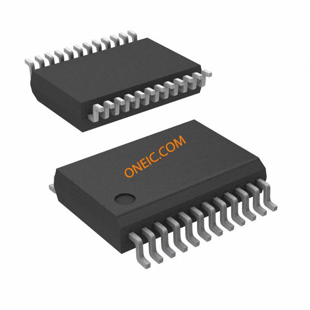
24-SSOP
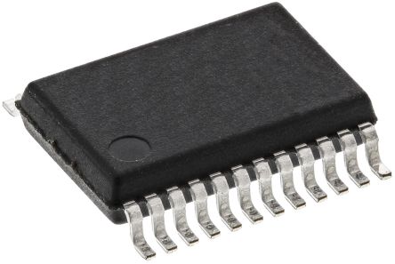
Image Preview
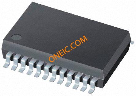
Image Preview