SN74LVC4245APW
Octal bus transceiver with voltage level shifting, 24-pin TSSOP package
Manufacturer: ['rochester', 'ti']
series introduction
# SN74LVC4245APW Product Series Introduction
## 1. Overview
The SN74LVC4245APW belongs to the SN74LVC4245A family of integrated circuits, which are high - performance, low - voltage, bidirectional octal bus transceivers. These devices are designed to provide efficient and reliable data transfer between two different buses in a wide range of electronic systems. They are well - suited for applications where low power consumption, high - speed operation, and compatibility with various logic levels are required.
## 2. Key Features
### 2.1 Low - Voltage Operation
- The SN74LVC4245APW is optimized for operation with a supply voltage (VCC) ranging from 1.65V to 3.6V. This low - voltage requirement makes it ideal for battery - powered devices, such as portable electronics, where power conservation is crucial. It helps to extend the battery life of the device while still maintaining high - performance operation.
### 2.2 Bidirectional Data Transfer
- One of the most significant features of this product series is its ability to perform bidirectional data transfer. It has eight independent data channels, allowing for the simultaneous transfer of 8 - bit data between two buses. The direction of data flow can be controlled using the DIR (Direction) input pin. This flexibility makes it suitable for applications where data needs to be transferred in both directions, such as in microcontroller - based systems, where data may need to be sent from the microcontroller to an external device and vice versa.
### 2.3 High - Speed Operation
- The SN74LVC4245APW offers high - speed data transfer capabilities. It has a typical propagation delay of around 3.8 ns (at VCC = 3.3V), which enables it to handle high - frequency data signals. This makes it suitable for applications that require fast data communication, such as in high - speed data acquisition systems or in communication interfaces like USB or Ethernet.
### 2.4 3 - State Outputs
- The outputs of the SN74LVC4245APW are 3 - state, which means they can be in one of three states: high, low, or high - impedance. The high - impedance state allows multiple devices to share the same bus without interfering with each other. When the OE (Output Enable) input is low, the outputs are enabled, and data is transferred between the two buses. When the OE input is high, the outputs are in the high - impedance state, effectively disconnecting the device from the bus.
### 2.5 Logic - Level Compatibility
- This product series is designed to be compatible with a wide range of logic levels. It can interface between different voltage domains, such as between a 1.8V microcontroller and a 3.3V peripheral device. The input thresholds are designed to accept both TTL and CMOS logic levels, providing greater flexibility in system design.
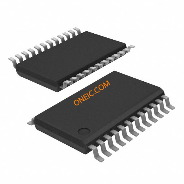
## 3. Package and Pin Configuration
### 3.1 Package Type
- The SN74LVC4245APW comes in a TSSOP (Thin Shrink Small Outline Package) package. This package is a surface - mount package that offers a compact form factor, making it suitable for applications where space is limited, such as in printed circuit boards (PCBs) of small - sized electronic devices.
### 3.2 Pin Configuration
- The device has a total of 20 pins. The pins are divided into power supply pins (VCC and GND), input/output pins for the two buses (A0 - A7 and B0 - B7), control pins (DIR and OE), and other necessary pins
Images for reference
24-TSSOP
Image Preview

Image Preview