SN74LVC4245ADBR
Octal bus transceivers with 3.3V to 5V level shifting in 24-pin SSOP format
Manufacturer: ['rochester', 'ti']
series introduction
# SN74LVC4245ADBR: A Comprehensive Introduction
## 1. Overview
The SN74LVC4245ADBR belongs to the SN74LVC4245A family of integrated circuits, which are high - performance, low - voltage, bidirectional octal bus transceivers. These devices are designed to provide efficient data transfer between two different data buses in a wide range of electronic systems. The "DBR" in the part number indicates the specific package type, which is a small outline integrated circuit (SOIC) with a 20 - lead configuration, making it suitable for surface - mount technology (SMT) assembly on printed circuit boards (PCBs).
## 2. Key Features
### 2.1 Low - Voltage Operation
- The SN74LVC4245ADBR is optimized for operation with a supply voltage range from 1.65V to 3.6V. This low - voltage requirement makes it ideal for battery - powered devices such as mobile phones, tablets, and portable media players, where power consumption is a critical factor. By operating at lower voltages, the device helps to extend the battery life of these products.
### 2.2 Bidirectional Data Transfer
- One of the most significant features of this transceiver is its ability to transfer data in both directions. It has two sets of eight - bit buses, labeled A and B. The direction of data flow between these two buses is controlled by a dedicated direction control (DIR) pin. When DIR is high, data is transferred from the A bus to the B bus, and when DIR is low, data is transferred from the B bus to the A bus. This bidirectional capability allows for flexible data communication between different parts of a system.
### 2.3 High - Speed Performance
- The SN74LVC4245ADBR offers high - speed data transfer rates, with typical propagation delays in the range of a few nanoseconds. This high - speed operation enables it to handle fast - paced data streams, making it suitable for applications such as high - speed data acquisition systems, communication interfaces, and digital signal processing.
### 2.4 3 - State Outputs
- Each of the output pins of the SN74LVC4245ADBR has a 3 - state output configuration. In addition to the normal high and low logic levels, the outputs can be placed in a high - impedance (Hi - Z) state. This is controlled by an output enable (OE) pin. When OE is low, the outputs are enabled, and data is transferred between the buses. When OE is high, the outputs are in the Hi - Z state, effectively disconnecting the device from the bus. This feature is useful for bus sharing applications, where multiple devices may be connected to the same bus, and only one device needs to drive the bus at a time.
### 2.5 Compatibility with Different Logic Levels
- The device is designed to be compatible with a variety of logic families. It can interface between different voltage levels, allowing for seamless communication between components operating at different supply voltages. For example, it can be used to connect a 1.8V microcontroller to a 3.3V peripheral device, ensuring proper data transfer between the two.
## 3. Functional Block Diagram and Pinout
### 3.1 Functional Block Diagram
- The SN74LVC4245ADBR consists of eight independent transceiver channels, each capable of bidirectional data transfer. The core of the device is the logic circuitry that controls the direction of data flow and the output enable function. The A and B buses are connected to the input/output pins of the transceiver channels, and the DIR and OE pins are used to control the
Images for reference
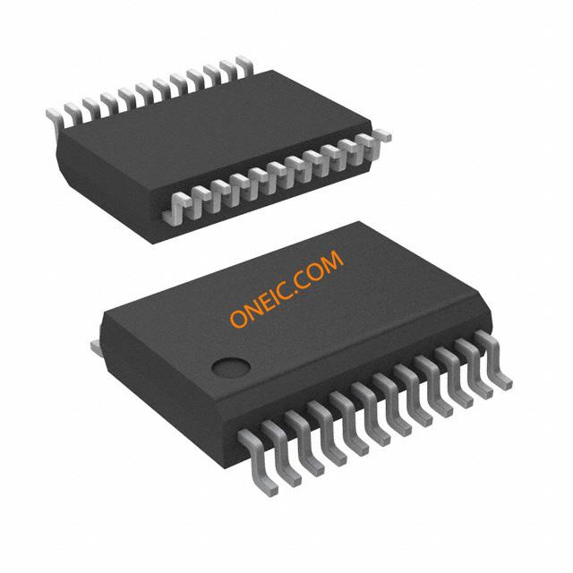
24-SSOP
Image Preview
Image Preview