SN74LVC374ADGVR
Dual and octal D-type flip-flops with edge-triggered and tri-state outputs
Manufacturer: ['rochester', 'analog-devices', 'ti']
series introduction
# SN74LVC374ADGVR Product Series Introduction
## 1. Overview
The SN74LVC374ADGVR belongs to the SN74LVC series of integrated circuits, which are widely recognized for their high - performance, low - power consumption, and compatibility with a variety of digital systems. This particular device, the SN74LVC374ADGVR, is an octal D - type flip - flop with 3 - state outputs, offering a reliable and efficient solution for data storage and transfer in digital circuits.
## 2. Key Features
### 2.1 Low - Voltage Operation
- The SN74LVC374ADGVR is designed to operate at low supply voltages, typically in the range of 1.65V to 3.6V. This low - voltage operation makes it suitable for battery - powered devices and other applications where power efficiency is crucial. It helps to reduce overall power consumption, extending the battery life of portable electronics such as smartphones, tablets, and handheld measurement devices.
### 2.2 High - Speed Performance
- With a high - speed data transfer rate, this flip - flop can handle rapid changes in input signals. It has a fast propagation delay, which allows for quick data storage and retrieval. This high - speed performance is essential in applications such as high - speed data communication systems, where real - time data processing is required.
### 2.3 3 - State Outputs
- The 3 - state outputs of the SN74LVC374ADGVR provide an additional level of flexibility. In the high - impedance state, the outputs are effectively disconnected from the circuit, allowing multiple devices to share the same data bus without interference. This feature is commonly used in bus - based systems, where multiple components need to communicate over a common data path.
### 2.4 Compatibility
- It is compatible with a wide range of logic families, including TTL (Transistor - Transistor Logic) and CMOS (Complementary Metal - Oxide - Semiconductor). This compatibility makes it easy to integrate the SN74LVC374ADGVR into existing digital circuits, reducing the need for complex level - shifting circuits.
### 2.5 ESD Protection
- The device is equipped with electrostatic discharge (ESD) protection, which helps to safeguard the internal circuitry from damage caused by static electricity. This protection is crucial in manufacturing environments and during normal use, as ESD events can occur easily and potentially destroy the device.
## 3. Functional Description
### 3.1 D - Type Flip - Flop Operation
- The SN74LVC374ADGVR consists of eight independent D - type flip - flops. Each flip - flop has a data input (D), a clock input (CP), and a clear input (CLR). When a rising edge is detected on the clock input (CP), the data present at the D input is transferred to the output (Q). The clear input (CLR) is an active - low input, which, when asserted, resets the output of all the flip - flops to a low state.
### 3.2 3 - State Output Control
- The 3 - state outputs are controlled by an output enable input (OE). When the OE input is low, the outputs are enabled, and the data stored in the flip - flops is presented at the outputs. When the OE input is high, the outputs enter the high - impedance state, effectively disconnecting them from the circuit.
## 4. Package and Pin Configuration
### 4.1 Package Type
- The SN74LVC374ADGVR is available in a small - outline integrated circuit (SOIC
Images for reference

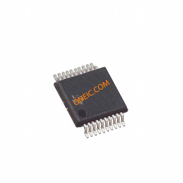
20-TVSOP Pkg

Image Preview

Image Preview