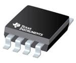
SN74LVC2G132DCUR
Dual 2-input NAND logic gates with Schmitt-trigger inputs
Manufacturer: ['rochester', 'ti']
series introduction
# SN74LVC2G132DCUR Product Series Introduction
## 1. Overview
The SN74LVC2G132DCUR belongs to the SN74LVC family of logic devices from Texas Instruments. This product series is specifically designed to offer high - performance, low - voltage operation in a compact form factor, making it an ideal choice for a wide range of digital circuit applications.
## 2. Key Features
### 2.1 Logic Function
The SN74LVC2G132DCUR is a dual 2 - input NAND Schmitt - trigger gate. The Schmitt - trigger input feature is crucial as it provides hysteresis, which means that the input switching thresholds are different for rising and falling edges. This helps in eliminating the effects of noise on the input signals, ensuring reliable operation even in noisy electrical environments. The NAND logic function is one of the fundamental building blocks in digital circuits, allowing for the implementation of more complex logic operations.
### 2.2 Low - Voltage Operation
It is designed to operate with a supply voltage range from 1.65V to 5.5V. This wide voltage range makes it highly versatile, as it can be easily integrated into different types of systems, whether they are low - power battery - operated devices or standard 5V logic systems. The low - voltage operation also contributes to reduced power consumption, which is a significant advantage in portable and energy - efficient applications.
### 2.3 High - Speed Performance
The device offers fast propagation delays, enabling it to handle high - frequency signals effectively. This high - speed performance is essential for applications where quick data processing and signal transmission are required, such as in communication systems and high - speed data buses.
### 2.4 Small Package Size
The SN74LVC2G132DCUR comes in a small SOT - 563 package. This compact package is beneficial for space - constrained applications, such as mobile devices, wearables, and other miniaturized electronic products. The small size also helps in reducing the overall board space requirements, which can lead to cost savings in the manufacturing process.
### 2.5 ESD Protection
It provides excellent electrostatic discharge (ESD) protection. The device can withstand ESD events up to ±2kV (Human - Body Model) and ±200V (Machine - Model). This protection ensures the reliability and durability of the device, especially in environments where ESD is a common concern, such as during handling and assembly processes.
## 3. Electrical Characteristics
### 3.1 Input and Output Voltage Levels
The input voltage levels are designed to be compatible with a wide range of logic families. The output voltage levels are well - defined, ensuring proper signal transfer between different components in a circuit. For example, the output high voltage (VOH) and output low voltage (VOL) are specified to meet the requirements of standard logic systems, allowing for seamless integration with other devices.
### 3.2 Power Consumption
The low - voltage operation of the SN74LVC2G132DCUR results in low power consumption. The quiescent current (ICC) is very low, which is especially important for battery - powered applications. This low power consumption helps in extending the battery life of portable devices and reduces the overall energy consumption of the system.
### 3.3 Drive Capability
The device has a sufficient drive capability to drive other logic gates or loads. The output current ratings (IOL and IOH) are specified to ensure that the device can provide the necessary current to drive the connected components without significant signal degradation.
## 4. Applications
### 4.1 Consumer Electronics
In mobile phones, tablets, and smartwatches, the SN74LVC2G1
Images for reference

US8_8_VSSOP_4200503_F

Image Preview