SN74LVC2G04DCKT
Dual inverter logic gates in compact SC-70 packages
Manufacturer: ['rochester', 'ti']
series introduction
# SN74LVC2G04DCKT Product Series Introduction
## 1. Overview
The SN74LVC2G04DCKT belongs to the Texas Instruments' SN74LVC family of logic devices. It is a dual inverter gate integrated circuit that offers high - performance and low - power operation, making it suitable for a wide range of digital applications. This product series is designed to meet the needs of modern electronic systems, providing reliable and efficient logic functions.
## 2. Key Features
### 2.1 Low - Voltage Operation
- The SN74LVC2G04DCKT is optimized for low - voltage operation, typically operating at supply voltages ranging from 1.65V to 5.5V. This wide voltage range allows it to be easily integrated into various systems with different power requirements, such as battery - powered devices where power conservation is crucial.
- Low - voltage operation also helps in reducing power consumption, which is beneficial for extending the battery life of portable electronics.
### 2.2 High - Speed Performance
- It offers high - speed switching characteristics, with typical propagation delays in the order of nanoseconds. This enables the device to handle high - frequency signals effectively, making it suitable for applications that require fast data processing and signal transmission, such as in communication systems and high - speed digital interfaces.
### 2.3 Low Power Consumption
- The LVC (Low - Voltage Complementary Metal - Oxide - Semiconductor) technology used in this product series results in extremely low power consumption. The quiescent current is very low, which is ideal for battery - operated devices and other power - sensitive applications. This low power consumption not only helps in reducing energy costs but also minimizes heat generation, improving the overall reliability of the system.
### 2.4 Compatibility
- The SN74LVC2G04DCKT is compatible with both TTL (Transistor - Transistor Logic) and CMOS (Complementary Metal - Oxide - Semiconductor) input levels. This compatibility allows it to interface easily with a wide variety of other logic devices, simplifying the design process of complex digital systems.
### 2.5 ESD Protection
- The device is equipped with excellent Electro - Static Discharge (ESD) protection. It can withstand high levels of ESD, which helps in preventing damage to the integrated circuit during handling, assembly, and normal operation. This protection enhances the reliability and durability of the product, especially in environments where ESD is a common concern.
## 3. Package and Pin Configuration
### 3.1 Package Type
The SN74LVC2G04DCKT comes in a small - outline no - lead (SON) package, specifically the DCKT package. This package offers several advantages, including a small footprint, which is beneficial for space - constrained applications such as mobile devices and compact circuit boards. The SON package also provides good thermal performance, allowing for efficient heat dissipation.
### 3.2 Pin Configuration
- The device has a total of 6 pins. Each of the two inverters has an input pin and an output pin. The power supply pin (VCC) and the ground pin (GND) are also provided. The clear and well - defined pin configuration makes it easy to connect the device to other components in a circuit.
## 4. Functional Description
### 4.1 Inverter Function
The SN74LVC2G04DCKT contains two independent inverter gates. An inverter, also known as a NOT gate, performs a logical inversion operation. That is, if the input signal is high (logic 1), the output signal will be low (logic 0), and vice versa. This basic logic function is fundamental in digital circuits and is used for tasks such as signal inversion,
Images for reference

SOT-363 PKG
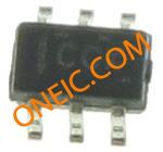
Image Preview

Image Preview