SN74LVC2G02DCUR
Dual 2-input positive NOR logic gates in compact 8-pin VSSOP format
Manufacturer: ['rochester', 'analog-devices', 'ti']
series introduction
# Introduction to the SN74LVC2G02DCUR Product Series
## 1. Overview
The SN74LVC2G02DCUR belongs to the Texas Instruments' SN74LVC family of low - voltage, high - speed complementary metal - oxide - semiconductor (CMOS) logic devices. This specific product is a dual 2 - input NOR gate, which is a fundamental building block in digital electronics. It is designed to operate at low voltages, making it suitable for a wide range of modern, battery - powered and low - power applications.
## 2. Key Features
### 2.1 Low - Voltage Operation
- The SN74LVC2G02DCUR can operate with a supply voltage (VCC) ranging from 1.65V to 5.5V. This wide voltage range allows it to be easily integrated into various systems, whether they are powered by a single - cell lithium - ion battery (around 3.7V) or a standard 5V power supply. Low - voltage operation also contributes to reduced power consumption, which is crucial for portable devices.
### 2.2 High - Speed Performance
- It offers high - speed switching characteristics. The propagation delay time is relatively short, typically in the range of a few nanoseconds. This enables the device to handle high - frequency digital signals, making it suitable for applications where fast data processing and signal propagation are required, such as in high - speed communication interfaces and digital signal processing circuits.
### 2.3 Compatibility
- The device is compatible with both TTL (Transistor - Transistor Logic) and CMOS logic levels. This means it can interface easily with other logic devices that use either TTL or CMOS standards, providing flexibility in system design. It can receive input signals from different types of logic circuits and drive loads that are compatible with these common logic families.
### 2.4 ESD Protection
- The SN74LVC2G02DCUR is equipped with electrostatic discharge (ESD) protection. It can withstand ESD events up to a certain level (e.g., ±2kV Human - Body Model (HBM) and ±200V Charged - Device Model (CDM)). This protection helps to prevent damage to the device during handling, assembly, and normal operation, increasing the reliability of the overall system.
### 2.5 Small Package Size
- It comes in a small - outline no - lead (SON) package, specifically the SOT - 563 package. The compact size of the package makes it ideal for applications where board space is limited, such as in mobile devices, wearables, and other miniaturized electronic products.
## 3. Functional Description
### 3.1 NOR Gate Function
- As a dual 2 - input NOR gate, the SN74LVC2G02DCUR has two independent NOR gates within a single package. A NOR gate performs the logical NOR operation, which means that the output of a NOR gate is HIGH (logic 1) only when both of its inputs are LOW (logic 0). Otherwise, the output is LOW.
- Mathematically, if we have two inputs A and B and an output Y, the logical expression for a NOR gate is \(Y=\overline{A + B}\), where the overbar represents the logical NOT operation and the plus sign represents the logical OR operation.
### 3.2 Input and Output Characteristics
- The input impedance of the device is relatively high, which means it draws very little current from the driving source. This is beneficial as it does not place a significant load on the previous stage of the circuit.
- The output of the NOR gate can drive a certain amount of load capacitance. The output current drive capability is specified in the datasheet, allowing
Images for reference

US8_8_VSSOP_4200503_F

Image Preview
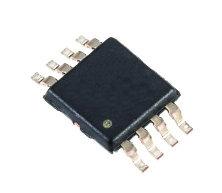
Image Preview