SN74LVC244ANSR
Octal buffer and line drivers with 3-state outputs for signal management
Manufacturer: ti
series introduction
# SN74LVC244ANSR Product Series Introduction
## 1. Overview
The SN74LVC244ANSR belongs to the SN74LVC series of integrated circuits, which are widely recognized for their high - performance and reliability in digital logic applications. This particular product, the SN74LVC244ANSR, is an octal buffer and line driver with 3 - state outputs. It is designed to provide efficient signal buffering and driving capabilities in various electronic systems, making it an essential component in modern digital circuit designs.
## 2. Key Features
### 2.1. Wide Voltage Range
- The SN74LVC244ANSR operates over a wide supply voltage range from 1.65V to 5.5V. This wide voltage tolerance allows it to be used in a variety of systems with different power supply requirements. For example, it can be integrated into low - power battery - operated devices that typically operate at lower voltages, as well as in more traditional 5V - based systems.
- This flexibility in voltage operation also enables seamless interfacing between different voltage domains within a complex electronic system, reducing the need for additional voltage - level conversion components.
### 2.2. High - Speed Performance
- It offers high - speed operation with typical propagation delays in the range of a few nanoseconds. This fast switching speed makes it suitable for applications where rapid data transfer and processing are required, such as in high - speed data buses, microprocessor interfaces, and communication systems.
- The ability to handle high - speed signals ensures that the device can keep up with the demanding clock frequencies of modern digital circuits, minimizing data transfer latency and improving overall system performance.
### 2.3. 3 - State Outputs
- The 3 - state outputs of the SN74LVC244ANSR provide an additional level of control. In the high - impedance (Hi - Z) state, the outputs are effectively disconnected from the circuit, allowing multiple devices to share the same bus without interfering with each other.
- This feature is crucial in bus - based systems, where multiple devices need to communicate over a common data path. By enabling or disabling the outputs of the SN74LVC244ANSR, the system can manage data flow and prevent bus contention, ensuring reliable data transfer.
### 2.4. Low Power Consumption
- The device is designed with low - power CMOS technology, which results in minimal power dissipation. This is especially important in battery - powered applications, where reducing power consumption extends the battery life of the device.
- Even in systems with continuous operation, the low power consumption helps to reduce heat generation, improving the overall reliability and longevity of the system by minimizing thermal stress on other components.
## 3. Functional Description
### 3.1. Pin Configuration
- The SN74LVC244ANSR comes in a small - outline no - lead (SON) package, which offers a compact form factor suitable for space - constrained applications. It has a total of 20 pins, which are carefully arranged to provide easy connection to other components in the circuit.
- The input pins are used to receive the digital signals that need to be buffered and driven, while the output pins deliver the amplified and conditioned signals. The enable pins control the operation of the 3 - state outputs, allowing the user to turn the outputs on or off as required.
### 3.2. Internal Circuitry
- Inside the SN74LVC244ANSR, there are eight independent buffer and driver circuits. Each circuit consists of a series of transistors and logic gates that are designed to amplify and shape the input signals.
- The internal circuitry is optimized to provide a high - quality output signal with minimal distortion and
Images for reference
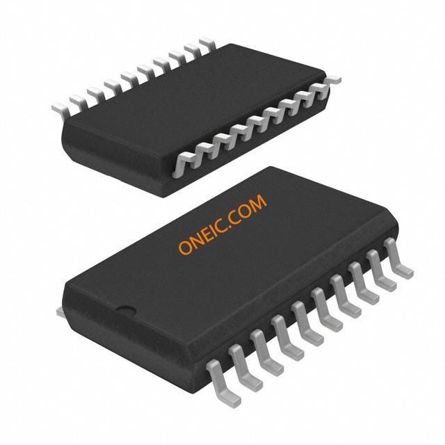
20-SOIC
Image Preview