SN74LVC1G80DBVR
Single positive-edge-triggered D-type flip-flop ICs in compact SOT-23 packages
Manufacturer: ['rochester', 'ti']
series introduction
# SN74LVC1G80DBVR Product Series Introduction
## 1. Overview
The SN74LVC1G80DBVR belongs to the Texas Instruments' SN74LVC family of single - gate logic devices. These single - gate components are designed to offer high - performance, low - power solutions for a wide range of digital applications. The SN74LVC1G80DBVR, in particular, is a single full - adder with carry output, which plays a crucial role in arithmetic operations within digital circuits.
## 2. Key Features
### 2.1 Low Voltage Operation
- It can operate over a wide voltage range, typically from 1.65V to 5.5V. This wide voltage tolerance makes it highly versatile, allowing it to be used in various power - supply environments. For example, in battery - powered devices where the supply voltage may vary as the battery discharges, the SN74LVC1G80DBVR can still function properly.
- Low - voltage operation also results in reduced power consumption, which is essential for portable and energy - efficient applications.
### 2.2 High - Speed Performance
- The device offers fast propagation delays, enabling it to handle high - frequency signals. This high - speed characteristic is beneficial in applications such as high - speed data processing and communication systems, where quick arithmetic operations are required.
- It can achieve propagation delays in the order of nanoseconds, ensuring that the addition operations are completed rapidly, minimizing the overall system latency.
### 2.3 Compatibility
- The SN74LVC1G80DBVR is compatible with both TTL (Transistor - Transistor Logic) and CMOS (Complementary Metal - Oxide - Semiconductor) input levels. This compatibility allows it to interface easily with a variety of other logic devices, simplifying the design process of complex digital circuits.
- It can be used in mixed - logic systems, where different types of logic families are combined to achieve specific functionality.
### 2.4 ESD Protection
- The device is equipped with excellent Electro - Static Discharge (ESD) protection. It can withstand ESD events up to a certain level, typically ±2kV Human - Body Model (HBM) and ±200V Charged - Device Model (CDM). This protection helps to prevent damage to the device during handling, assembly, and normal operation, increasing its reliability and lifespan.
## 3. Functional Description
### 3.1 Full - Adder Functionality
- The SN74LVC1G80DBVR performs the function of a single full - adder. A full - adder is a combinational logic circuit that adds three one - bit binary numbers: two input bits (A and B) and a carry - in bit (Cin). It produces two output bits: a sum bit (S) and a carry - out bit (Cout).
- The truth table of the full - adder shows all possible combinations of the input bits and the corresponding output bits. For example, when A = 0, B = 0, and Cin = 0, S = 0 and Cout = 0; when A = 1, B = 1, and Cin = 1, S = 1 and Cout = 1.
### 3.2 Logic Diagram
- The internal logic of the SN74LVC1G80DBVR consists of a combination of basic logic gates such as AND, OR, and XOR gates. These gates are interconnected in a specific way to implement the full - adder functionality.
- The input pins A, B, and Cin are connected to the appropriate logic gates, and the output pins S and Cout are the results of the logical operations performed by the internal circuitry.
Images for reference
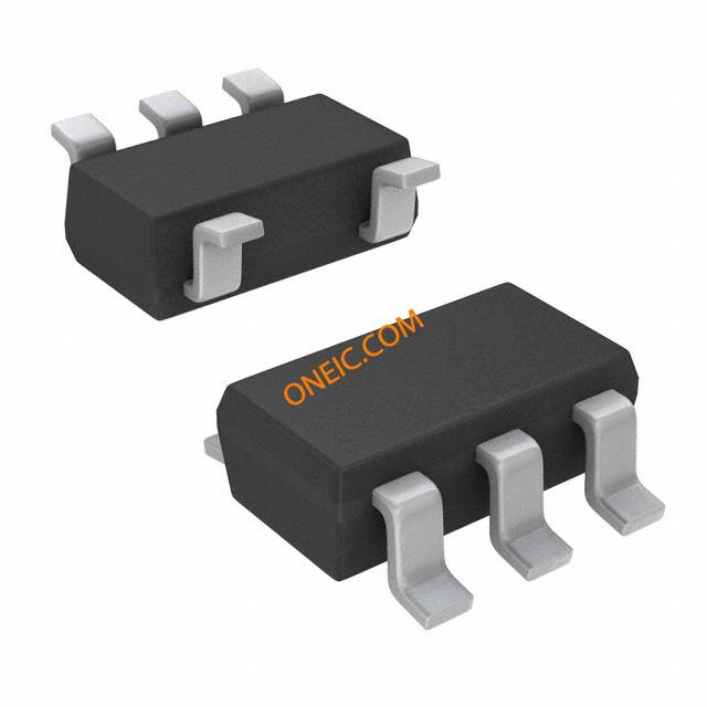
SOT-23-5, SC-74A
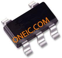
Image Preview
Image Preview