SN74LVC1G07MDCKREP
Single-channel non-inverting CMOS buffer/driver with open-drain output
Manufacturer: ti
series introduction
# SN74LVC1G07MDCKREP Product Series Introduction
## 1. Overview
The SN74LVC1G07MDCKREP belongs to the Texas Instruments' SN74LVC family of single - gate logic devices. This product series is designed to offer high - performance, low - voltage operation in a compact package, making it an ideal choice for a wide range of applications in modern electronic systems.
## 2. Key Features
### 2.1 Low - Voltage Operation
- The SN74LVC1G07MDCKREP is optimized for operation with a supply voltage range from 1.65V to 5.5V. This wide voltage range allows it to be easily integrated into various systems, whether they are powered by low - voltage batteries or standard power supplies. For example, in portable devices where power efficiency is crucial, the ability to operate at lower voltages helps to extend battery life.
### 2.2 High - Speed Performance
- It provides fast propagation delays, enabling rapid signal processing. The typical propagation delay is in the order of a few nanoseconds, which is essential for applications that require high - speed data transfer and processing. This makes it suitable for use in high - frequency communication systems, such as wireless transceivers, where quick signal handling is necessary to maintain data integrity.
### 2.3 Rail - to - Rail Input and Output
- The device supports rail - to - rail input and output capabilities. This means that the input voltage can swing from the ground level (0V) up to the supply voltage (VCC), and the output can also reach these extreme levels. Rail - to - rail operation simplifies the interface design between different components in a circuit, as it allows for direct connection without the need for additional level - shifting circuitry.
### 2.4 Low Power Consumption
- With its low - power design, the SN74LVC1G07MDCKREP consumes minimal power during operation. This is particularly beneficial for battery - powered devices, as it helps to reduce overall power consumption and increase the device's runtime. In addition, low power consumption also leads to less heat generation, which can improve the reliability and longevity of the device.
### 2.5 ESD Protection
- The product is equipped with electrostatic discharge (ESD) protection. It can withstand high - voltage ESD events, typically up to ±2kV (Human Body Model), which helps to prevent damage to the device during handling and operation. This protection feature is crucial in environments where ESD is a common concern, such as in manufacturing facilities or when the device is exposed to static - prone materials.
## 3. Package and Pin Configuration
### 3.1 Package Type
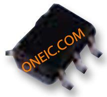
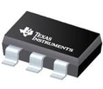
- The SN74LVC1G07MDCKREP comes in a small - outline no - lead (SON) package, specifically the SOT - 563 package. This package offers several advantages, including a small footprint, which is beneficial for space - constrained applications. The SON package also provides good thermal performance, allowing for efficient heat dissipation from the device.
### 3.2 Pin Configuration
- The device has a simple pin configuration. It typically has an input pin, an output pin, a power supply pin (VCC), and a ground pin (GND). The clear and straightforward pin layout makes it easy to integrate into a circuit board, reducing the complexity of the design process.
## 4. Functional Description
### 4.1 Logic Function
- The SN74LVC1G07MDCKREP is a single - gate buffer with open - drain output. A buffer is a circuit that simply passes the input signal to the output with minimal distortion. The open - drain output allows for easy
Images for reference

74LVC Series (SC70)

Image Preview

Image Preview