SN74LVC1G04MDBVREP
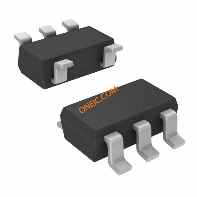
Single inverter gate ICs in compact SOT-23-5 package
Manufacturer: ti
series introduction
# SN74LVC1G04MDBVREP: A Comprehensive Introduction
## 1. Overview
The SN74LVC1G04MDBVREP is a member of the SN74LVC series of single - gate logic devices from Texas Instruments. This product is designed to offer high - performance, low - voltage operation in a compact package, making it an ideal choice for a wide range of applications in modern electronic systems.
## 2. Key Features
### 2.1 Low - Voltage Operation
- It operates over a wide voltage range, typically from 1.65V to 5.5V. This wide voltage tolerance allows it to be used in various power - supply environments, whether it's a low - power battery - operated device or a standard 5V system. For example, in a portable sensor device powered by a single lithium - ion battery (around 3.7V), the SN74LVC1G04MDBVREP can function effectively without the need for complex voltage - conversion circuits.
### 2.2 High - Speed Performance
- With a high - speed propagation delay, it can handle fast - changing input signals. The typical propagation delay is in the order of a few nanoseconds. This makes it suitable for applications where quick signal processing is required, such as in high - speed data communication interfaces or clock - distribution networks. For instance, in a USB 2.0 data line, where data transfer rates can reach up to 480 Mbps, the device can keep up with the rapid signal transitions.
### 2.3 Low Power Consumption
- The device is designed with low - power CMOS technology. It has very low static and dynamic power consumption, which is crucial for battery - powered devices. In standby mode, the quiescent current is extremely low, helping to extend the battery life of portable electronics. For example, in a wireless earbud, where power efficiency is of utmost importance, the SN74LVC1G04MDBVREP can contribute to longer usage times between charges.
### 2.4 ESD Protection
- It provides excellent electrostatic discharge (ESD) protection. The device can withstand ESD events up to a certain level (e.g., ±2kV Human - Body Model (HBM) and ±200V Charged - Device Model (CDM)). This protection helps to prevent damage to the device during handling, assembly, and normal operation, increasing the reliability of the overall system.
### 2.5 Small Package Size
- The SN74LVC1G04MDBVREP comes in a small - outline package, such as the SOT - 353. This compact package is beneficial for space - constrained applications, allowing for high - density circuit board designs. In a smartwatch, where every square millimeter of the printed circuit board (PCB) is precious, the small package of this device enables more components to be integrated into a limited space.
## 3. Functional Description
### 3.1 Logic Function
- The SN74LVC1G04MDBVREP is a single inverter gate. It takes an input signal and produces an inverted output signal. That is, if the input is a logic high (e.g., close to the supply voltage), the output will be a logic low (close to ground), and vice versa. This basic logic function is fundamental in digital circuits and can be used for tasks such as signal inversion, level shifting, and creating simple logic combinations.
### 3.2 Input and Output Characteristics
- The input impedance of the device is very high, which means it draws very little current from the driving source. This is important as it minimizes the loading effect on the previous stage of the circuit. The
Images for reference

SOT-23-5, SC-74A

Image Preview

Image Preview