SN74LVC08ADBR
Quad 2-input AND logic gates in 14-pin SSOP for versatile electronic circuits
Manufacturer: ['rochester', 'ti']
series introduction
# SN74LVC08ADBR Product Series Introduction
## 1. Overview
The SN74LVC08ADBR belongs to the SN74LVC series of integrated circuits, which are widely recognized for their high - performance, low - power consumption, and compatibility with a variety of digital systems. This specific product, the SN74LVC08ADBR, is a quad 2 - input AND gate, designed to perform basic logical AND operations in digital circuits. It is packaged in a small - outline no - lead (SON) package, which offers several advantages in terms of space - saving and electrical performance.
## 2. Key Features
### 2.1 Electrical Characteristics
- **Low Voltage Operation**: The SN74LVC08ADBR can operate within a wide voltage range, typically from 1.65V to 5.5V. This wide voltage tolerance makes it suitable for use in a variety of power - supply environments, including battery - powered devices where lower voltages are common.
- **Low Power Consumption**: It is designed with low - power CMOS technology, which results in very low static and dynamic power dissipation. This is crucial for applications where power efficiency is a priority, such as portable electronics and battery - operated systems.
- **High - Speed Operation**: Despite its low - power design, the device can achieve high - speed operation with typical propagation delays in the range of a few nanoseconds. This allows it to be used in high - frequency digital circuits where fast signal processing is required.
### 2.2 Input and Output Compatibility
- **TTL and CMOS Compatibility**: The inputs of the SN74LVC08ADBR are compatible with both TTL (Transistor - Transistor Logic) and CMOS (Complementary Metal - Oxide - Semiconductor) logic levels. This means it can interface easily with a wide range of other digital components, providing flexibility in system design.
- **Output Drive Capability**: The outputs of the device can drive a significant load, with a typical output current of several milliamperes. This allows it to directly drive other logic gates or small - scale integrated circuits without the need for additional buffering in many cases.
### 2.3 Package and Physical Characteristics
- **SON Package**: The SN74LVC08ADBR comes in a SON package, which is a surface - mount package with a small footprint. This makes it ideal for applications where board space is limited, such as in mobile devices, wearables, and other compact electronic products.
- **Thermal Performance**: The SON package also offers good thermal performance, allowing the device to dissipate heat efficiently. This helps to ensure reliable operation even under high - temperature conditions.
## 3. Functional Description
### 3.1 Logical Operation
As a quad 2 - input AND gate, the SN74LVC08ADBR has four independent AND gates, each with two inputs and one output. The output of an AND gate is high (logic 1) only when both of its inputs are high. Otherwise, the output is low (logic 0). This basic logical operation is fundamental in digital circuit design and is used in a wide variety of applications, such as data processing, control systems, and signal conditioning.
### 3.2 Pin Configuration
The device has a specific pin configuration that is designed for easy integration into printed circuit boards (PCBs). The pins are clearly labeled for the inputs, outputs, power supply, and ground, making it straightforward for designers to connect the device to other components in the circuit.
## 4. Applications
### 4.1 Digital Logic Circuits
The SN74LVC08ADBR is commonly used in digital logic circuits to perform logical AND operations. It can be used in combination with other logic
Images for reference
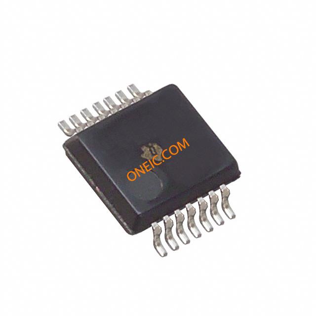
14-SSOP Pkg
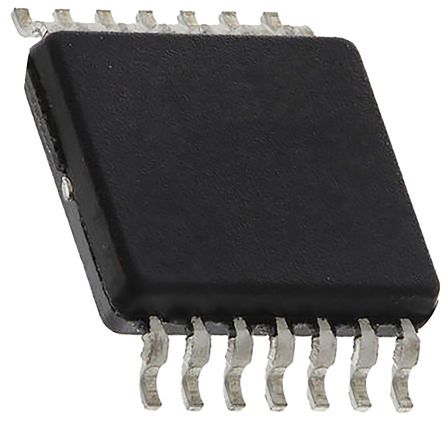
Image Preview
Image Preview