SN74LS74ADR
Dual positive-edge-triggered D-type flip-flops with preset and clear functionality
Manufacturer: ti
series introduction
# Introduction to the SN74LS74ADR Product Series
## 1. Overview
The SN74LS74ADR belongs to the 74LS series of integrated circuits, which are well - known for their reliability and wide range of applications in digital electronics. Specifically, the SN74LS74ADR is a dual D - type positive - edge - triggered flip - flop with preset and clear inputs. It is a surface - mount device (SMD) packaged in a small outline integrated circuit (SOIC) package, which is suitable for modern printed circuit board (PCB) designs that require high - density component placement.
## 2. Key Features
### 2.1 Electrical Characteristics
- **Power Supply Range**: It operates within a power supply voltage range of 4.75V to 5.25V, which is in line with the standard TTL (Transistor - Transistor Logic) power requirements. This makes it compatible with many other TTL - based components in a digital system.
- **Low Power Consumption**: The LS (Low - power Schottky) technology used in this device significantly reduces power consumption compared to traditional TTL devices. This is beneficial for battery - powered applications or systems where power efficiency is a concern.
- **Fast Propagation Delay**: The device has relatively fast propagation delays, typically in the range of a few nanoseconds. This allows for high - speed operation, making it suitable for applications that require quick data processing and signal transfer.
### 2.2 Functional Features
- **Dual D - Type Flip - Flops**: The SN74LS74ADR contains two independent D - type flip - flops in a single package. Each flip - flop has a data input (D), a clock input (CLK), a preset input (PRE), a clear input (CLR), and a complementary output (Q and Q̅).
- **Positive - Edge - Triggered**: The flip - flops are triggered on the positive edge of the clock signal. This means that the data present at the D input is transferred to the Q output only when the clock signal makes a low - to - high transition. This edge - triggering mechanism helps in synchronizing the data transfer with the system clock, reducing the chances of data errors.
- **Preset and Clear Functions**: The preset (PRE) and clear (CLR) inputs are active - low. When the PRE input is pulled low, the Q output is set to a high state regardless of the D input and the clock signal. Similarly, when the CLR input is pulled low, the Q output is cleared to a low state. These functions are useful for initializing the flip - flops or for forcing a specific output state during system operation.
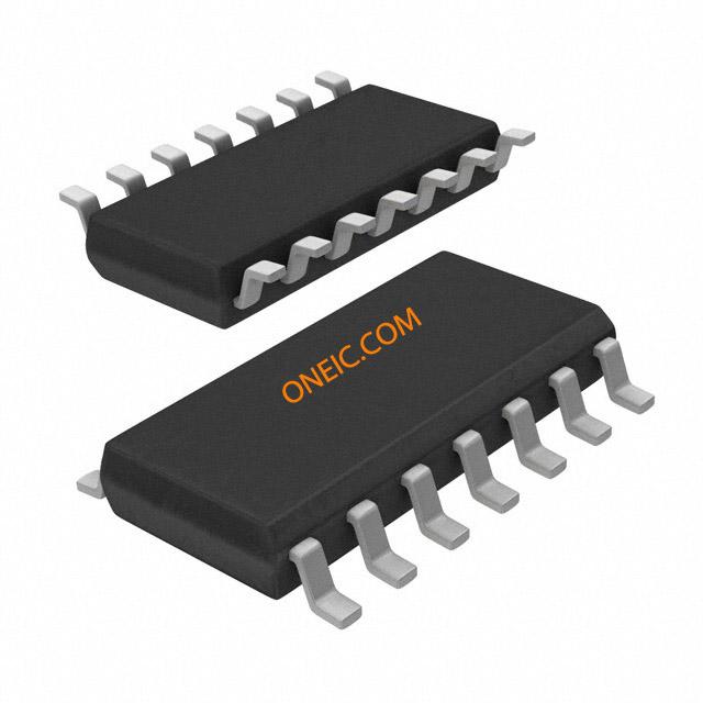
## 3. Package and Pinout
### 3.1 Package
The SN74LS74ADR comes in a SOIC - 14 package. The SOIC package is a popular choice for surface - mount applications due to its small size, which allows for compact PCB designs. It has a standard pitch between the pins, making it easy to place and solder on the PCB using automated assembly equipment.
### 3.2 Pinout
- **Pin 1 (1CLR)**: Clear input for the first flip - flop (active - low).
- **Pin 2 (1D)**: Data input for the first flip - flop.
- **Pin 3 (1CLK)**: Clock input for the first flip - flop.
- **Pin 4 (1PRE)**: Preset input for the first flip - flop (active - low).
- **Pin 5 (1Q)**: Output of the first flip - flop.
- **Pin 6 (1Q̅
Images for reference

14-SOIC
14-TSSOPa
Image Preview