SN74LS05DBR
Hex inverter ICs with open collector outputs in 14-pin SSOP format
Manufacturer: ['rochester', 'analog-devices', 'ti']
series introduction
# Introduction to the SN74LS05DBR Product Series
## 1. Overview
The SN74LS05DBR belongs to the 74LS (Low - Power Schottky) series of integrated circuits, which are widely recognized for their reliability, performance, and cost - effectiveness in digital logic applications. This specific product is a hex inverter with open - collector outputs, offering a versatile solution for various digital circuit designs.
## 2. Key Features
### 2.1 Electrical Characteristics
- **Low Power Consumption**: The LS technology in SN74LS05DBR is designed to consume less power compared to standard TTL (Transistor - Transistor Logic) devices. This makes it suitable for battery - powered applications or systems where power efficiency is a critical concern. For example, in portable measurement devices or small - scale embedded systems, the reduced power consumption helps to extend the battery life.
- **High - Speed Operation**: It can operate at relatively high speeds, with typical propagation delays in the range of a few nanoseconds. This allows for fast signal processing and is essential in applications such as high - speed data communication systems, where quick response times are required to ensure accurate data transfer.
### 2.2 Output Configuration
- **Open - Collector Outputs**: The open - collector outputs of the SN74LS05DBR provide flexibility in circuit design. An open - collector output can be used to drive loads that require a specific voltage level or to interface with other devices that have different voltage requirements. For instance, it can be used to drive LEDs, relays, or to create a wired - AND connection in a digital circuit. When used to drive an LED, the open - collector output can sink current from the LED, allowing for easy control of the LED's illumination.
### 2.3 Compatibility
- **TTL Compatibility**: The SN74LS05DBR is fully compatible with TTL logic levels. This means that it can be easily integrated into existing TTL - based systems without the need for additional level - shifting circuitry. It can directly interface with other TTL devices such as microcontrollers, memory chips, and other logic gates, simplifying the design process and reducing the overall cost of the system.
## 3. Package and Pinout
### 3.1 Package Type
The SN74LS05DBR comes in a small - outline integrated circuit (SOIC) package. The SOIC package is a surface - mount package that offers several advantages, including a smaller footprint compared to through - hole packages. This makes it suitable for printed circuit board (PCB) designs where space is limited, such as in modern consumer electronics and compact industrial control systems.
### 3.2 Pinout
The device has 14 pins, with each of the six inverters having an input and an output pin. The power supply pins (VCC and GND) are also clearly defined. The pinout is standardized, which makes it easy for designers to incorporate the SN74LS05DBR into their circuit layouts. For example, the input pins are typically labeled A1 - A6, and the corresponding output pins are labeled Y1 - Y6, following a logical and consistent naming convention.
## 4. Applications
### 4.1 Signal Inversion
The primary function of the SN74LS05DBR is signal inversion. In digital circuits, there are often requirements to invert the logic level of a signal. For example, in a microcontroller - based system, the output of a sensor may need to be inverted before it can be processed by the microcontroller. The SN74LS05DBR can perform this inversion task efficiently, ensuring that the signal is in the correct logic state for further processing.
### 4.2 Level Shifting and Interface
Images for reference
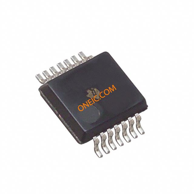
14-SSOP Pkg
Image Preview
Image Preview