SN74HCT245PW
Octal bus transceivers with 3-state outputs in 20-pin TSSOP packages
Manufacturer: ['rochester', 'analog-devices', 'ti']
series introduction
# SN74HCT245PW Product Series Introduction
## 1. Overview
The SN74HCT245PW is a part of the Texas Instruments' 74HCT logic family, which is widely recognized for its high - performance and reliability in digital circuit applications. This particular product is an octal bus transceiver with 3 - state outputs, designed to provide bidirectional data transfer between two buses. It is an essential component in many electronic systems, enabling efficient communication and data handling.
## 2. Key Features
### 2.1 Compatibility
- **TTL and CMOS Compatibility**: The SN74HCT245PW is designed to interface between TTL (Transistor - Transistor Logic) and CMOS (Complementary Metal - Oxide - Semiconductor) logic systems. It can accept TTL - level input signals and provide CMOS - level output signals, making it highly versatile in mixed - logic environments. This compatibility allows designers to integrate different types of logic circuits seamlessly, reducing the complexity of system design.
- **Supply Voltage Range**: It operates over a wide supply voltage range of 4.5V to 5.5V. This flexibility in power supply requirements makes it suitable for a variety of applications, from battery - powered devices to more traditional power - hungry systems.
### 2.2 High - Speed Operation
- **Fast Propagation Delay**: The device has a relatively short propagation delay, typically in the range of a few nanoseconds. This high - speed operation enables it to handle high - frequency data signals, making it ideal for applications where real - time data transfer is crucial, such as in high - speed data communication systems and microprocessor - based systems.
### 2.3 3 - State Outputs
- **Bidirectional Control**: The 3 - state outputs of the SN74HCT245PW can be controlled to be in either a high - impedance (Hi - Z) state, a logic high state, or a logic low state. The direction of data flow between the two buses (A and B) can be controlled by a dedicated direction control input (DIR). When the output enable input (OE) is active low, the device allows data to flow in the direction specified by the DIR input. When OE is high, the outputs are placed in the high - impedance state, effectively disconnecting the device from the buses. This feature is essential for bus sharing in multi - device systems, as it allows multiple devices to share the same bus without interfering with each other.
### 2.4 Low Power Consumption
- **CMOS Technology**: Being based on CMOS technology, the SN74HCT245PW consumes relatively low power compared to some other logic families. This low power consumption is beneficial for battery - powered devices, as it helps to extend the battery life. It also reduces the overall power dissipation in the system, which can lead to lower operating temperatures and increased reliability.
## 3. Pin Configuration and Functionality
### 3.1 Pinout
The SN74HCT245PW is available in a 20 - pin TSSOP (Thin Shrink Small Outline Package) or other package options. The pins are divided into several groups:
- **Power Pins**: VCC (pin 20) is the positive power supply pin, and GND (pin 10) is the ground pin.
- **Data Pins**: There are two sets of eight data pins each. Pins 1 - 8 are the A - bus pins (A1 - A8), and pins 11 - 18 are the B - bus pins (B1 - B8). These pins are used for bidirectional data transfer between the two buses.
- **Control Pins**:
- Output Enable
Images for reference
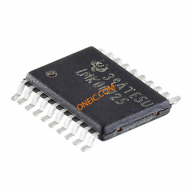
LMK00725PW
Image Preview

Image Preview