SN74HC573ADW
Octal D-type transparent latches with 3-state outputs in 20-pin SOIC
Manufacturer: ['rochester', 'ti']
series introduction
# SN74HC573ADW Product Series Introduction
## 1. Overview
The SN74HC573ADW belongs to the SN74HC573 family of octal transparent D-type latches. These integrated circuits are designed to store and transfer digital data in a wide range of electronic systems. The "SN" is the Texas Instruments (TI) product prefix, "74HC" indicates the high - speed CMOS logic family, "573" is the specific device number for this octal latch, and "ADW" represents the package type.
## 2. Key Features
### Electrical Characteristics
- **Wide Supply Voltage Range**: It can operate with a supply voltage (VCC) ranging from 2 V to 6 V. This wide range makes it suitable for use in various power - supply environments, whether in battery - powered devices or systems with a standard 5 V power source.
- **Low Power Consumption**: As a member of the CMOS family, it consumes very low power compared to traditional TTL (Transistor - Transistor Logic) devices. This is especially important in portable and battery - operated applications where power efficiency is crucial.
- **High - Speed Operation**: The high - speed nature of the HC family allows for fast data transfer. It has typical propagation delays in the range of a few nanoseconds, enabling it to handle high - frequency digital signals and support rapid data processing.
### Logic Functionality
- **Octal Design**: The SN74HC573ADW contains eight independent D - type latches. Each latch has a data input (D), an output enable (OE) input, and a latch enable (LE) input. This octal configuration makes it convenient for handling 8 - bit data buses commonly used in microcontrollers, memory systems, and other digital circuits.
- **Transparent Latching**: When the latch enable (LE) input is high, the outputs (Q) follow the data inputs (D). When LE goes low, the data present at the inputs at that moment are latched, and the outputs retain those values until LE goes high again. This transparent latching feature provides flexibility in data storage and transfer operations.
- **Output Enable Control**: The output enable (OE) input is used to control whether the latched data is presented at the outputs. When OE is low, the latched data appears at the outputs. When OE is high, the outputs are in a high - impedance state, effectively disconnecting them from the circuit.
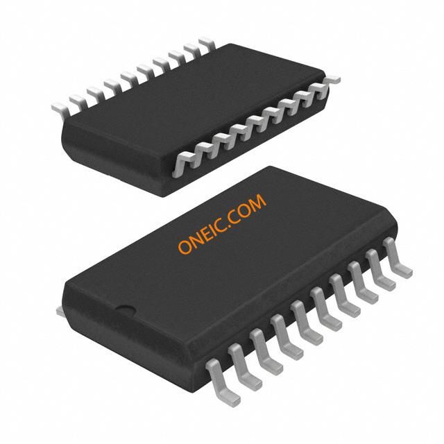
## 3. Package and Pinout
### Package Type
The "ADW" in the part number indicates that the device comes in a small - outline integrated circuit (SOIC) package. The SOIC package is a surface - mount package that is widely used in modern printed circuit board (PCB) designs. It offers a compact form factor, which is beneficial for space - constrained applications.
### Pinout
- **Data Inputs (D0 - D7)**: These eight pins are used to input the digital data that will be latched.
- **Outputs (Q0 - Q7)**: The corresponding eight pins provide the latched data when the output enable (OE) is active.
- **Latch Enable (LE)**: A single pin that controls the latching operation. When LE is high, the outputs follow the inputs; when low, the data is latched.
- **Output Enable (OE)**: This pin controls whether the latched data is presented at the outputs. A low level on OE enables the outputs, while a high level puts them in a high - impedance state.
- **Power Supply Pins**: VCC is the positive power supply pin, and GND is the ground pin.
## 4. Applications
### Microcontroller Systems
In micro
Images for reference

20-SOIC 0.295
20-SOIC 0.295
Image Preview