SN74HC541PWR
8-bit non-inverting buffers with tri-state outputs in TSSOP packaging
Manufacturer: ti
series introduction
# SN74HC541PWR Product Series Introduction
## 1. Overview
The SN74HC541PWR is a part of the Texas Instruments' SN74HC series, which is well - known for its high - speed CMOS technology. This particular device, the SN74HC541PWR, is an octal buffer/line driver with 3 - state outputs. It is designed to provide high - performance buffering and driving capabilities for a wide range of digital systems, making it an essential component in many electronic applications.
## 2. Key Features
### 2.1 High - Speed Operation
The HC (High - Speed CMOS) technology used in the SN74HC541PWR enables it to achieve fast propagation delays. This high - speed operation is crucial in applications where rapid data transfer is required, such as in high - speed data buses, microprocessor systems, and communication interfaces. It can handle clock frequencies in the tens of megahertz range, ensuring that data can be processed and transmitted quickly and efficiently.
### 2.2 3 - State Outputs
One of the most significant features of the SN74HC541PWR is its 3 - state outputs. In addition to the standard high and low logic states, the outputs can be placed in a high - impedance (Hi - Z) state. This allows multiple devices to be connected to a common bus without interfering with each other. When a device's outputs are in the Hi - Z state, it effectively disconnects from the bus, enabling other devices to communicate freely. This feature is essential in bus - based systems, where multiple components need to share the same communication line.
### 2.3 Wide Supply Voltage Range
The SN74HC541PWR can operate over a wide supply voltage range, typically from 2 V to 6 V. This flexibility makes it suitable for use in a variety of power - supply environments. It can be easily integrated into systems with different power requirements, whether it is a low - voltage battery - powered device or a standard 5 V logic system.
### 2.4 Low Power Consumption
Despite its high - speed operation, the SN74HC541PWR consumes relatively low power. This is due to the CMOS technology, which has inherently low static power consumption. The low power consumption makes it an ideal choice for battery - powered devices, where power efficiency is a critical factor. It helps to extend the battery life of portable electronics and reduces the overall power requirements of the system.
### 2.5 Compatibility
The SN74HC541PWR is compatible with both TTL (Transistor - Transistor Logic) and CMOS logic levels. This means that it can interface easily with other TTL or CMOS devices in a system. It simplifies the design process and allows for seamless integration with existing components, reducing the need for additional level - shifting circuits.
## 3. Pin Configuration and Functionality
### 3.1 Pinout
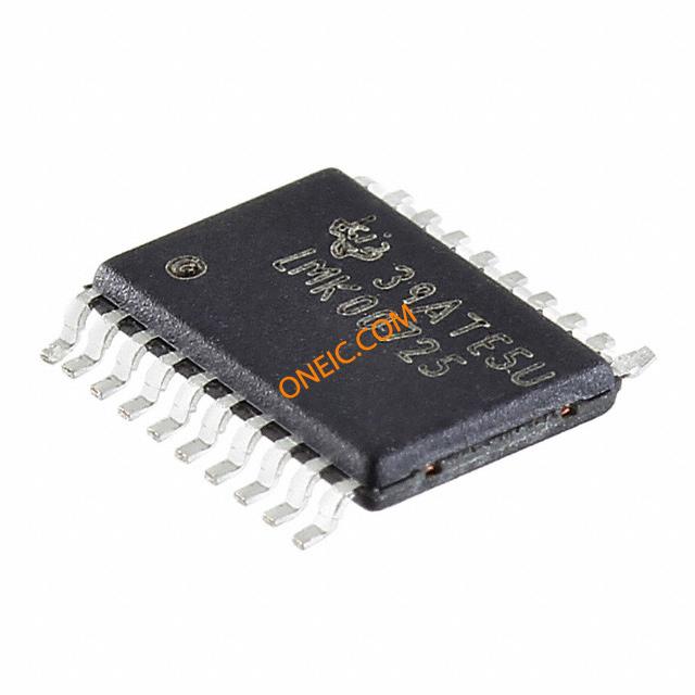
The SN74HC541PWR is available in a TSSOP (Thin Shrink Small Outline Package) with 20 pins. The pins are divided into input pins, output pins, control pins, and power supply pins.
- **Input Pins (A0 - A7)**: These pins are used to receive the input signals. The data to be buffered or driven is applied to these pins.
- **Output Pins (Y0 - Y7)**: The buffered and driven output signals are available at these pins. The output logic state is determined by the input signal and the state of the control pins.
- **Control Pins**: There are two control pins, \(\overline{OE1}\) and \(\overline{OE2}\). These are active -
Images for reference
LMK00725PW
Image Preview

Image Preview