SN74HC4851D
Single 8:1 analog multiplexer/demultiplexer ICs in 16-pin SOIC/TVSOP packages
Manufacturer: ['rochester', 'analog-devices', 'ti']
series introduction
# SN74HC4851D Product Series Introduction
## 1. Overview
The SN74HC4851D belongs to the SN74HC series of integrated circuits, which are well - known for their high - speed CMOS technology. This product series is specifically designed as a 2 - input multiplexer/demultiplexer, offering a versatile solution for signal routing and selection in various digital electronic systems.
## 2. Key Features
### 2.1 High - Speed Operation
The HC (High - Speed CMOS) technology employed in the SN74HC4851D enables it to operate at relatively high clock frequencies. This high - speed performance makes it suitable for applications where rapid signal processing and switching are required, such as in high - speed data communication systems and fast - paced digital control circuits.
### 2.2 Low Power Consumption
CMOS technology is inherently known for its low power consumption characteristics. The SN74HC4851D consumes minimal power during normal operation, which is a significant advantage in battery - powered devices or systems where power efficiency is crucial. This helps in reducing overall energy costs and extending the battery life of portable electronics.
### 2.3 Wide Operating Voltage Range
The device can operate over a wide voltage range, typically from 2 V to 6 V. This wide voltage tolerance allows it to be easily integrated into different types of electronic systems with varying power supply requirements. Whether it is a low - voltage microcontroller - based system or a standard 5V logic circuit, the SN74HC4851D can function effectively.
### 2.4 Compatibility with TTL Logic
The SN74HC4851D is designed to be compatible with TTL (Transistor - Transistor Logic) levels. This means that it can interface seamlessly with other TTL - based components in a mixed - logic system. It simplifies the design process when integrating the device into existing TTL - dominated circuits, as there is no need for complex level - shifting circuitry.
## 3. Functional Description
### 3.1 Multiplexer Function
As a multiplexer, the SN74HC4851D has the ability to select one of two input signals and route it to the output. The selection is controlled by a select input pin. When the select input is in a particular logic state, one of the input signals is passed through to the output, while the other input is effectively ignored. This functionality is useful in applications where multiple data sources need to be shared on a single output line, such as in data acquisition systems where different sensors' data need to be sequentially processed.
### 3.2 Demultiplexer Function
In the demultiplexer mode, the SN74HC4851D takes a single input signal and distributes it to one of two output lines based on the state of the select input. This is beneficial in scenarios where a single control signal needs to be routed to different parts of a circuit depending on certain conditions, for example, in a control system where a single command needs to be sent to different actuators based on the system's state.
## 4. Pin Configuration
The SN74HC4851D is typically available in a small - outline integrated circuit (SOIC) package. The pinout is carefully designed to provide easy access to all the necessary input and output signals.
- **Input Pins**: There are two data input pins (A and B) that carry the signals to be multiplexed or demultiplexed. The select input pin (S) determines which input is selected in multiplexer mode or which output the input is routed to in demultiplexer mode.
- **Output Pin**: There is a single output pin (Y) in multiplexer mode, and two output pins
Images for reference

16 SOIC

16-TVSOP
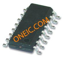
Image Preview