SN74HC14PWG4
Hex Schmitt-trigger inverters in 14-pin TSSOP for signal conditioning
Manufacturer: ti
series introduction
# SN74HC14PWG4 Product Series Introduction
## 1. Overview
The SN74HC14PWG4 belongs to the SN74HC series of integrated circuits, which are well - known for their high - performance and reliability in digital logic applications. This specific product is a hex inverter with Schmitt - trigger inputs. It combines the functionality of an inverter with the unique characteristics of Schmitt - trigger inputs, making it suitable for a wide range of digital and analog interface applications.
## 2. Key Features
### 2.1 Schmitt - Trigger Inputs
The most prominent feature of the SN74HC14PWG4 is its Schmitt - trigger inputs. Schmitt - trigger circuits have two different threshold voltages for rising and falling edges. When the input voltage rises, it must cross the upper threshold voltage ($V_{T+}$) to cause a change in the output state. When the input voltage falls, it must cross the lower threshold voltage ($V_{T -}$) to change the output state again. This hysteresis effect makes the device highly resistant to noise. In noisy environments, small voltage fluctuations around the normal switching threshold will not cause false triggering, ensuring stable and reliable operation of the circuit.
### 2.2 High - Speed Operation
The HC (High - Speed CMOS) technology used in the SN74HC14PWG4 enables high - speed signal processing. It has a relatively short propagation delay, which means that it can quickly respond to changes in the input signal. This high - speed characteristic is crucial in applications where fast data transfer and processing are required, such as in high - speed communication systems and digital signal processing circuits.
### 2.3 Wide Supply Voltage Range
The device can operate over a wide supply voltage range, typically from 2 V to 6 V. This flexibility allows it to be used in various power supply configurations, making it compatible with different types of systems. Whether it is a low - voltage battery - powered device or a standard 5 V logic system, the SN74HC14PWG4 can be easily integrated.
### 2.4 Low Power Consumption
As a CMOS - based device, the SN74HC14PWG4 has low power consumption. CMOS technology only draws significant current during the switching transitions, and in the static state, the power consumption is extremely low. This makes it an ideal choice for battery - powered devices and other applications where power efficiency is a critical factor.
## 3. Pin Configuration and Functionality
### 3.1 Pinout
The SN74HC14PWG4 is typically available in a small - outline package (SOIC) or a thin - shrink small - outline package (TSSOP). It has 14 pins, with each pin having a specific function:
- **Power Pins**: Pin 7 is the ground (GND) pin, and pin 14 is the positive power supply ($V_{CC}$) pin. These pins provide the necessary electrical power for the operation of the device.
- **Input and Output Pins**: There are six pairs of input and output pins. For example, pin 1 is an input pin, and pin 2 is the corresponding output pin. The input signals are inverted at the output according to the logic function of the inverter.
### 3.2 Logic Function
The basic logic function of each inverter in the SN74HC14PWG4 is to invert the input signal. That is, when the input is a logic high (close to $V_{CC}$), the output is a logic low (close to GND), and vice versa. The Schmitt - trigger action ensures that the input signal is properly conditioned before the inversion takes place, providing a clean and stable output.
## 4. Applications
Images for reference
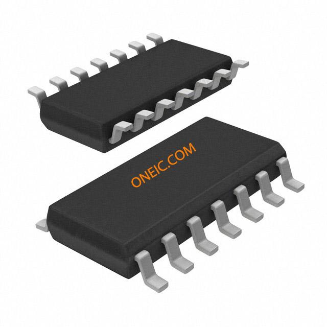
14-TSSOPa
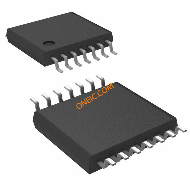
14-TSSOP
Image Preview