SN74HC10N
Triple 3-input NAND logic gates in 14-pin PDIP/SOP packages
Manufacturer: ['rochester', 'ti']
series introduction
# SN74HC10N Product Series Introduction
## 1. Overview
The SN74HC10N belongs to the 74HC series of integrated circuits, which are high - speed CMOS logic devices. These devices combine the high - speed operation characteristics of TTL (Transistor - Transistor Logic) with the low power consumption of CMOS (Complementary Metal - Oxide - Semiconductor) technology. The SN74HC10N specifically is a triple 3 - input NAND gate integrated circuit, widely used in digital logic circuits for various applications.
## 2. Key Features
### 2.1 Electrical Characteristics
- **Power Supply Range**: The SN74HC10N can operate within a relatively wide power supply voltage range, typically from 2V to 6V. This flexibility allows it to be used in different power supply environments, whether in battery - powered low - voltage systems or standard 5V logic circuits.
- **Low Power Consumption**: Thanks to its CMOS technology, the device consumes very little power in both static and dynamic states. In standby mode, the quiescent current is extremely low, making it suitable for battery - operated devices where power efficiency is crucial.
- **High - Speed Operation**: It offers high - speed switching performance, with propagation delays typically in the range of a few nanoseconds. This enables it to handle high - frequency digital signals, making it suitable for applications that require fast data processing and signal transmission.
### 2.2 Input and Output Characteristics
- **Input Compatibility**: The inputs of the SN74HC10N are compatible with both TTL and CMOS logic levels. This means it can interface easily with other logic devices from different families, providing great flexibility in circuit design.
- **Output Drive Capability**: The outputs can drive a certain number of standard loads. They can source and sink a reasonable amount of current, typically up to 4mA at a 5V power supply, which is sufficient to drive other logic gates or small - scale loads directly.
### 2.3 Noise Immunity
CMOS technology gives the SN74HC10N good noise immunity. It can tolerate a certain amount of noise on the input signals without causing false triggering, ensuring the reliability of the digital circuit in noisy environments.
## 3. Pin Configuration
The SN74HC10N is available in a standard 14 - pin dual - in - line package (DIP). The pin configuration is as follows:
- **Pins 1, 2, 3**: Inputs of the first 3 - input NAND gate. Pin 1 is input A1, pin 2 is input B1, and pin 3 is input C1.
- **Pin 4**: Output of the first 3 - input NAND gate (Y1).
- **Pins 5, 6, 8**: Inputs of the second 3 - input NAND gate. Pin 5 is input A2, pin 6 is input B2, and pin 8 is input C2.
- **Pin 7**: Ground (GND).
- **Pin 9**: Output of the second 3 - input NAND gate (Y2).
- **Pins 10, 11, 12**: Inputs of the third 3 - input NAND gate. Pin 10 is input A3, pin 11 is input B3, and pin 12 is input C3.
- **Pin 13**: Output of the third 3 - input NAND gate (Y3).
- **Pin 14**: Positive power supply (VCC).
## 4. Functional Description
A NAND gate is a fundamental digital logic gate. The output
Images for reference
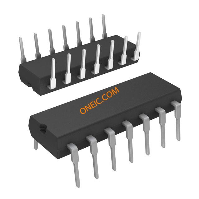
14-DIP
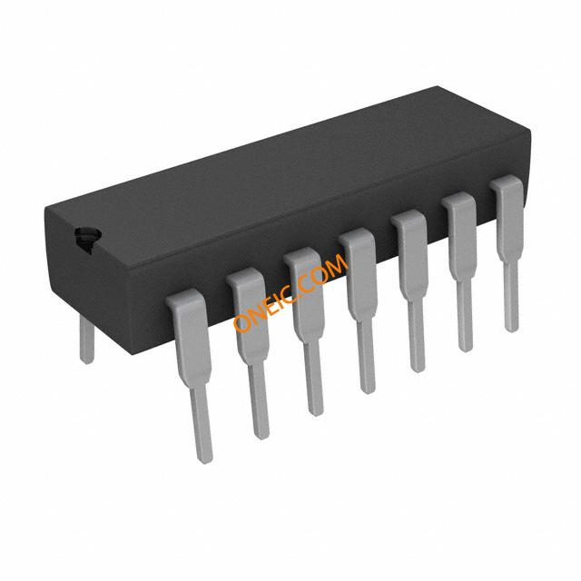
14-Dip
Image Preview