SN74F138N
3-to-8 line decoder/demultiplexer ICs in various 16-pin packages
Manufacturer: ['rochester', 'ti']
series introduction
# SN74F138N Product Series Introduction
## 1. Overview
The SN74F138N belongs to the 74F series of integrated circuits, which are part of the high - speed TTL (Transistor - Transistor Logic) family. This specific device, the SN74F138N, is a 3 - to - 8 line decoder/demultiplexer. Decoders and demultiplexers are fundamental building blocks in digital electronics, used for a wide range of applications from address decoding in memory systems to signal routing in communication circuits.
## 2. Key Features
### 2.1 High - Speed Operation
One of the most significant features of the SN74F138N is its high - speed performance. The 'F' in the 74F series stands for fast. It has a typical propagation delay time that is much shorter compared to standard TTL devices. This makes it suitable for applications where quick response times are crucial, such as in high - speed microprocessor systems where address decoding needs to be done rapidly to access memory or peripheral devices.
### 2.2 Low Power Consumption
Despite its high - speed operation, the SN74F138N is designed to consume relatively low power. This is achieved through advanced semiconductor manufacturing processes and circuit design techniques. Low power consumption is beneficial in battery - powered devices or in large - scale systems where reducing overall power consumption can lead to cost savings and improved thermal management.
### 2.3 Compatibility
The SN74F138N is compatible with other TTL - level devices. It can interface easily with a wide range of digital integrated circuits, including microcontrollers, microprocessors, and other logic gates. This compatibility simplifies the design process of complex digital systems, as designers can mix and match different components from the TTL family without having to worry about significant signal - level mismatches.
### 2.4 Multiple Enable Inputs
The device has three enable inputs (two active - low and one active - high). These enable inputs provide a high degree of flexibility in controlling the operation of the decoder. By using these enable inputs, the decoder can be selectively activated or disabled based on the system requirements. For example, in a multi - module system, different decoders can be enabled or disabled at different times to manage the flow of data and control signals.
## 3. Pin Configuration
### 3.1 Input Pins
- **A0, A1, A2**: These are the three address input pins. The binary combination of the signals on these pins determines which of the eight output lines will be activated. For example, if A0 = 0, A1 = 0, and A2 = 0, the output line Y0 will be selected.
- **G1**: This is an active - high enable input. The decoder will only operate when a high - level signal is applied to this pin.
- **G2A, G2B**: These are active - low enable inputs. The decoder will function only when both of these pins are at a low - level signal.
### 3.2 Output Pins
- **Y0 - Y7**: These are the eight output lines. Only one of these lines will be driven low (active - low output) at a time, depending on the combination of the address inputs and the state of the enable inputs.
### 3.3 Power and Ground Pins
- **VCC**: This pin is connected to the positive power supply voltage. For the SN74F138N, the typical operating voltage is +5V.
- **GND**: This pin is connected to the ground reference.
## 4. Functional Description
### 4.1 Decoder Operation
As a
Images for reference
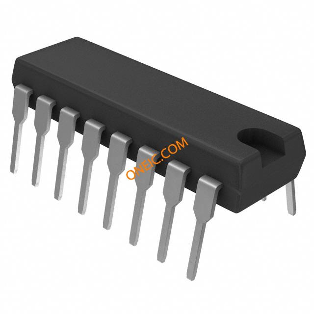
16-DIP SOT38-1
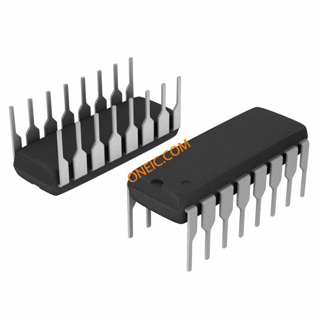
16-Dip
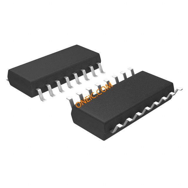
16-SOIC