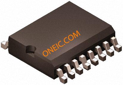
SN74CBT3257DR
Quad 2:1 multiplexer/demultiplexer ICs in 16-pin SOIC packaging
Manufacturer: ['rochester', 'analog-devices', 'ti']
series introduction
# SN74CBT3257DR Product Series Introduction
## 1. Overview
The SN74CBT3257DR belongs to a family of high - performance analog and digital switch integrated circuits. These devices are designed to provide efficient signal routing and switching capabilities in a wide range of electronic applications. Texas Instruments, a well - known semiconductor manufacturer, produces the SN74CBT3257DR, leveraging its expertise in semiconductor technology to ensure high - quality and reliable performance.
## 2. Key Features
### 2.1 Low On - Resistance
One of the standout features of the SN74CBT3257DR is its low on - resistance. This characteristic is crucial as it minimizes signal attenuation and power loss when the switch is in the on state. Low on - resistance ensures that the integrity of the transmitted signals is maintained, making it suitable for applications where signal quality is of utmost importance, such as high - speed data transmission and precision analog signal routing.
### 2.2 Wide Supply Voltage Range
The device supports a wide supply voltage range, typically from 2 V to 5.5 V. This flexibility allows it to be used in various power - supply environments, whether it's a low - voltage battery - powered device or a standard 5 V logic system. It simplifies the design process as designers can integrate the SN74CBT3257DR into different types of circuits without having to worry about strict power - supply requirements.
### 2.3 High - Speed Switching
With fast switching times, the SN74CBT3257DR can handle high - frequency signals effectively. It can quickly transition between the on and off states, enabling seamless signal routing in applications that require rapid signal switching, such as in communication systems where data needs to be routed between different channels in a short period.
### 2.4 Bidirectional Operation
The SN74CBT3257DR supports bidirectional signal flow. This means that signals can be transmitted in either direction through the switch, providing greater flexibility in circuit design. It can be used to connect two different parts of a circuit in a way that allows for two - way communication, which is useful in applications like data buses and audio signal routing.
### 2.5 ESD Protection
The device is equipped with electrostatic discharge (ESD) protection. ESD can cause damage to electronic components, especially in sensitive circuits. The built - in ESD protection in the SN74CBT3257DR helps safeguard the device from static electricity, increasing its reliability and longevity in real - world applications.
## 3. Pin Configuration and Functionality
### 3.1 Pinout
The SN74CBT3257DR comes in a small - outline integrated circuit (SOIC) package with a specific pin configuration. The pins are divided into different categories, including power supply pins, control pins, and signal input/output pins.
- **Power Supply Pins**: These pins are used to provide the necessary power to the device. The VCC pin is connected to the positive power supply, while the GND pin is connected to the ground.
- **Control Pins**: The control pins are used to control the state of the switches. By applying appropriate logic levels to these pins, the user can turn the switches on or off, thereby controlling the signal routing.
- **Signal Input/Output Pins**: These pins are used to connect the external circuits to the switches. Signals can be input through these pins and routed to the appropriate output pins based on the state of the switches.
### 3.2 Functionality
The operation of the SN74CBT3257DR is controlled by the logic levels applied to the control pins. When the control pins are set to the appropriate logic levels
Images for reference

16 SOIC

Image Preview

Image Preview