SN74ALVC164245DGGR
16-bit voltage level shifting transceiver with tri-state outputs
Manufacturer: ['rochester', 'ti', 'nxp']
series introduction
# SN74ALVC164245DGGR: A Comprehensive Product Series Introduction
## 1. Overview
The SN74ALVC164245DGGR belongs to the SN74ALVC164245 family of integrated circuits. It is a high - performance, 16 - bit bus transceiver designed to provide bidirectional voltage - level translation and buffering capabilities. This product series is widely used in various digital systems where efficient data transfer between different voltage domains is required.
## 2. Key Features
### 2.1 Voltage - Level Translation
- **Wide Voltage Range**: The SN74ALVC164245DGGR supports voltage - level translation between two different power - supply voltages. It can operate with VCCA (Port A supply voltage) ranging from 1.65V to 3.6V and VCCB (Port B supply voltage) also ranging from 1.65V to 3.6V. This flexibility allows it to interface between different logic families and devices operating at different voltage levels, such as between a 1.8V microcontroller and a 3.3V peripheral.
- **Bi - directional Translation**: It can translate data in both directions, enabling seamless communication between two voltage - incompatible systems. For example, data can be transferred from a low - voltage source on Port A to a high - voltage destination on Port B, and vice versa.
### 2.2 High - Speed Operation
- **Fast Propagation Delay**: The device has a very low propagation delay, which means it can transfer data quickly. This is crucial in high - speed digital systems where data needs to be processed and transferred in a timely manner. For instance, in high - speed data acquisition systems or high - frequency communication interfaces, the low propagation delay ensures that data is not significantly delayed during transmission.
- **High - Frequency Compatibility**: It can operate at high frequencies, making it suitable for applications that require fast data transfer rates. This allows it to keep up with the demands of modern digital systems, such as high - speed serial interfaces and high - performance microprocessors.
### 2.3 Low Power Consumption
- **Power - Saving Design**: The SN74ALVC164245DGGR is designed with low - power CMOS technology. This results in reduced power consumption compared to traditional bipolar logic devices. In battery - powered applications, such as portable electronics, the low power consumption helps to extend the battery life.
- **Power - Down Mode**: It also features a power - down mode, which further reduces power consumption when the device is not in use. This is useful in systems where power management is critical, such as in energy - efficient IoT devices.
### 2.4 ESD Protection
- **Robust ESD Protection**: The product is equipped with electrostatic discharge (ESD) protection on all inputs and outputs. This protection helps to prevent damage to the device from static electricity, which is a common problem in electronic systems. It enhances the reliability and durability of the device, especially in environments where static electricity is likely to occur, such as in industrial or consumer electronics.
## 3. Functional Description
### 3.1 Pin Configuration
The SN74ALVC164245DGGR comes in a specific pin - out package. It has two sets of 16 - bit data ports (Port A and Port B), along with control pins. The control pins include the direction control (DIR) pin, which determines the direction of data flow between Port A and Port B, and the output enable (OE) pin, which enables or disables the outputs of the device.
### 3.2 Data Transfer Operation
- **Direction Control**: When the DIR pin is set to a high logic level,
Images for reference

48-TSSOP
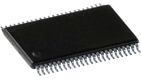
Image Preview
Image Preview