SN74AHCT367DR
Hex non-inverting buffer and line drivers with tri-state outputs
Manufacturer: ti
series introduction
# SN74AHCT367DR Product Series Introduction
## 1. Overview
The SN74AHCT367DR belongs to the SN74AHCT series of integrated circuits produced by Texas Instruments. This specific product is a high - speed hex buffer/driver with 3 - state outputs. It is designed to provide a reliable and efficient solution for signal buffering and driving in a wide range of digital electronic applications.
## 2. Key Features
### 2.1 High - Speed Operation
- The SN74AHCT367DR is built with advanced semiconductor technology that enables high - speed signal propagation. It has a typical propagation delay time in the order of nanoseconds. This high - speed performance makes it suitable for applications where fast data transfer and processing are required, such as in high - speed data buses and communication systems.
### 2.2 3 - State Outputs
- One of the most significant features of this device is its 3 - state outputs. In addition to the standard high and low logic states, the outputs can be placed in a high - impedance (Hi - Z) state. This feature allows multiple devices to share a common bus without interfering with each other. When the output is in the Hi - Z state, it effectively disconnects from the bus, enabling other devices to drive the bus signals.
### 2.3 Compatibility
- It is designed to be compatible with both TTL (Transistor - Transistor Logic) and CMOS (Complementary Metal - Oxide - Semiconductor) logic levels. This compatibility makes it easy to interface with a variety of other digital components, whether they are based on TTL or CMOS technology. It can be used in mixed - technology systems without the need for additional level - shifting circuits in many cases.
### 2.4 Low Power Consumption
- The SN74AHCT367DR is optimized for low power consumption. This is achieved through the use of advanced CMOS technology, which reduces the static and dynamic power dissipation of the device. Low power consumption is crucial in battery - powered applications and systems where energy efficiency is a priority, as it helps to extend the battery life and reduce overall power consumption.
## 3. Pin Configuration and Functionality
### 3.1 Pinout
- The SN74AHCT367DR is typically available in a small - outline integrated circuit (SOIC) package with 16 pins. The pins are divided into input pins, output pins, control pins, and power supply pins.
- **Input Pins**: There are six input pins (A1 - A6) that receive the input signals. These signals are buffered and then driven to the corresponding output pins.
- **Output Pins**: Six output pins (Y1 - Y6) provide the buffered and driven versions of the input signals. The state of these output pins depends on the input signals and the control signals.
- **Control Pins**: There are two active - low output enable pins (OE1 and OE2). When these pins are low, the outputs are enabled, and the input signals are passed through to the outputs. When either of these pins is high, the outputs are placed in the high - impedance state.
- **Power Supply Pins**: The device requires a single power supply voltage (VCC) and a ground connection (GND). The recommended power supply voltage range is typically from 4.5V to 5.5V, which is compatible with standard 5V digital systems.
### 3.2 Functionality
- The basic functionality of the SN74AHCT367DR is to buffer and drive the input signals to the output pins. When the output enable pins are active (low), the logic level at the input pins is replicated at the corresponding output
Images for reference

16 SOIC

Image Preview
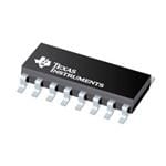
Image Preview