SN74AHC595PW
8-bit shift registers with serial/parallel conversion in TSSOP/SOIC packages
Manufacturer: ['rochester', 'ti']
series introduction
# SN74AHC595PW Product Series Introduction
## 1. Overview
The SN74AHC595PW is a highly versatile and widely - used integrated circuit belonging to the Texas Instruments' SN74AHC series. It is an 8 - bit serial - in, parallel - out shift register with a storage register and three - state outputs. This device is designed to expand the number of output pins of a microcontroller or other digital control systems, making it an essential component in various digital electronics applications.
## 2. Key Features
### 2.1 Serial - to - Parallel Conversion
One of the primary features of the SN74AHC595PW is its ability to convert serial data into parallel data. This is extremely useful when a microcontroller has limited parallel output pins. By sending data serially to the shift register, the device can then present the data in parallel form at its output pins. This simplifies the wiring and reduces the number of control lines required in a circuit.
### 2.2 Storage Register
The device incorporates a storage register. This allows the data that has been shifted into the shift register to be latched and held stable at the output. The storage register can be updated independently of the shift register, providing flexibility in controlling when the output data is changed.
### 2.3 Three - State Outputs
The SN74AHC595PW has three - state outputs. This means that the outputs can be in one of three states: high, low, or high - impedance. The high - impedance state effectively disconnects the output from the rest of the circuit, which is useful in applications where multiple devices share the same bus. It allows for easy multiplexing and sharing of resources.
### 2.4 High - Speed Operation
The AHC (Advanced High - Speed CMOS) technology used in this device enables high - speed operation. It has a fast propagation delay, which means that data can be shifted and latched quickly. This makes it suitable for applications that require rapid data transfer and processing, such as high - speed display systems and real - time control circuits.
### 2.5 Wide Operating Voltage Range
The SN74AHC595PW can operate over a wide voltage range, typically from 2 V to 5.5 V. This makes it compatible with a variety of power supplies and digital systems. It can be easily integrated into both low - voltage and standard 5 - V systems, providing flexibility in different design scenarios.
## 3. Pin Configuration
### 3.1 Input Pins
- **SER (Serial Data Input)**: This pin is used to input serial data into the shift register. Data is shifted into the register one bit at a time on the rising edge of the shift clock.
- **SRCLK (Shift Register Clock)**: The rising edge of this clock signal shifts the data from the SER pin into the shift register. Each rising edge moves the data one bit position further into the register.
- **RCLK (Storage Register Clock)**: A rising edge on this pin transfers the data from the shift register to the storage register. This effectively updates the parallel outputs of the device.
- **SRCLR (Shift Register Clear)**: A low logic level on this pin clears the contents of the shift register, resetting all the bits to zero.
- **OE (Output Enable)**: A low logic level on this pin enables the three - state outputs, allowing the data from the storage register to appear at the output pins. A high logic level puts the outputs in the high - impedance state.
### 3.2 Output Pins
- **Q0 - Q7**: These are the 8 parallel output pins of the device. The data stored in the storage register is presented at these pins when the output is enabled
Images for reference
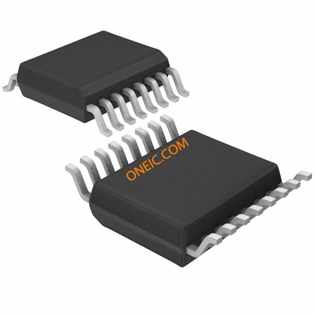
16-TSSOP

Image Preview
Image Preview