SN74AHC1G08DBV
Single 2-input AND gate logic IC in compact SOT-23 package
Manufacturer: ['rochester', 'ti']
series introduction
# SN74AHC1G08DBV Product Series Introduction
## 1. Overview
The SN74AHC1G08DBV belongs to the Texas Instruments' SN74AHC family of logic devices. It is a single 2 - input AND gate integrated circuit, designed to offer high - performance logic functionality in a compact and efficient package. This product series is widely used in various electronic applications where space - saving and reliable logic operations are crucial.
## 2. Key Features
### Electrical Characteristics
- **Wide Supply Voltage Range**: The SN74AHC1G08DBV can operate with a supply voltage (VCC) ranging from 2 V to 5.5 V. This wide range makes it compatible with a variety of power sources and allows for seamless integration into different electronic systems, whether they are powered by low - voltage batteries or standard power supplies.
- **Low Power Consumption**: It features low static and dynamic power consumption. In standby mode, the quiescent current is extremely low, which is beneficial for battery - powered devices as it helps to extend the battery life. During normal operation, the dynamic power consumption is also optimized, reducing overall power dissipation and heat generation.
- **High - Speed Operation**: With a typical propagation delay of just a few nanoseconds, this AND gate can handle high - frequency signals. It can operate at clock frequencies up to several tens of megahertz, enabling it to be used in high - speed digital circuits such as data communication systems and microprocessor - based applications.
### Logic Functionality
- **2 - Input AND Gate**: The core function of the SN74AHC1G08DBV is to perform the logical AND operation on its two input signals. The output of the AND gate is high (logic 1) only when both of its inputs are high. Otherwise, the output is low (logic 0). This basic logic function is fundamental in digital circuit design and is used for tasks such as signal masking, data filtering, and control signal generation.
- **Buffered Output**: The output of the AND gate is buffered, which means it can drive a certain amount of load without significant signal degradation. This allows the device to be connected to other logic gates or components in a circuit without the need for additional buffering stages in many cases.
### Package and Physical Characteristics
- **Small - Outline Package**: The SN74AHC1G08DBV comes in a small - outline SOT - 23 package. This package is very compact, with a small footprint on the printed circuit board (PCB). It is suitable for applications where space is limited, such as mobile devices, wearable electronics, and other miniaturized electronic products.
- **RoHS Compliance**: The product is compliant with the Restriction of Hazardous Substances (RoHS) directive. This means that it does not contain harmful substances such as lead, mercury, cadmium, and certain flame retardants, making it environmentally friendly and suitable for use in products that need to meet strict environmental regulations.
## 3. Applications
### Consumer Electronics
- **Mobile Phones and Tablets**: In mobile devices, the SN74AHC1G08DBV can be used for signal processing and control functions. For example, it can be used to combine control signals from different components, such as the power management unit and the touchscreen controller, to ensure proper operation of the device.
- **Wearable Devices**: Due to its small size and low power consumption, it is an ideal choice for wearable electronics like smartwatches and fitness trackers. It can be used in sensor interfaces to process and filter sensor data, or in power management circuits to control the power supply to different modules.
### Industrial Automation
- **PLC (Programmable Logic Controller) Systems**: In industrial control
Images for reference
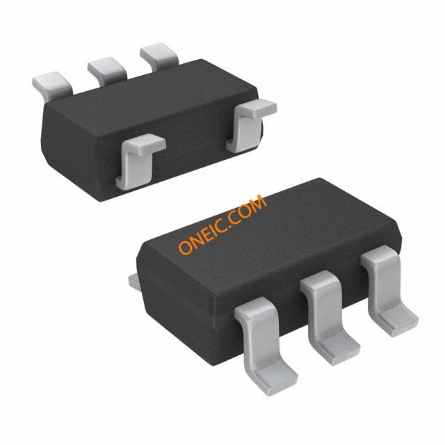
SOT-23-5, SC-74A
Image Preview
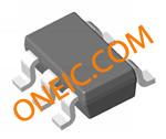
Image Preview