SN74ACT244DBR
Octal buffer and line driver ICs with 3-state outputs in SSOP package
Manufacturer: ['onsemi', 'rochester', 'ti']
series introduction
# SN74ACT244DBR Product Series Introduction
## 1. Overview
The SN74ACT244DBR is a part of the Texas Instruments' 74ACT logic family, which is well - known for its high - performance and reliability in digital circuit applications. This particular device is an octal buffer and line driver with 3 - state outputs, designed to provide efficient signal buffering and driving capabilities in various digital systems.
## 2. Key Features
### 2.1 High - Speed Operation
- The SN74ACT244DBR is built using advanced CMOS technology, enabling it to operate at high speeds. It has a typical propagation delay of around 6 ns, which makes it suitable for applications where fast signal processing is required, such as high - speed data communication systems and real - time control circuits.
### 2.2 3 - State Outputs
- One of the most significant features of this device is its 3 - state outputs. The 3 - state outputs can be in one of three states: high, low, or high - impedance. In the high - impedance state, the output is effectively disconnected from the circuit, allowing multiple devices to share a common bus without interfering with each other. This feature is crucial in bus - based systems, where multiple components need to communicate over a shared data path.
### 2.3 Wide Operating Voltage Range
- It can operate over a wide voltage range from 4.5 V to 5.5 V. This flexibility in power supply voltage makes it compatible with a variety of power sources and other components in a system. It also allows for easy integration into existing designs that may have different power requirements.
### 2.4 Low Power Consumption
- Despite its high - speed operation, the SN74ACT244DBR consumes relatively low power. This is due to the use of CMOS technology, which has lower static power consumption compared to other logic families. Low power consumption is beneficial in battery - powered devices and applications where energy efficiency is a priority.
## 3. Pin Configuration and Functionality
### 3.1 Pinout
- The SN74ACT244DBR comes in a small - outline integrated circuit (SOIC) package with 20 pins. The pins are divided into input pins, output pins, enable pins, and power supply pins.
- There are two groups of four buffers each. Each group has its own active - low enable input (OE1# and OE2#). When the enable input is low, the corresponding group of buffers is enabled, and the input signals are passed through to the output. When the enable input is high, the outputs of the corresponding group are in the high - impedance state.
### 3.2 Input and Output Characteristics
- The inputs of the SN74ACT244DBR are designed to accept TTL - compatible logic levels. This means that it can be easily interfaced with other TTL - based devices. The outputs are capable of driving standard loads, such as other logic gates or transmission lines. They can source and sink sufficient current to ensure reliable signal transmission.
## 4. Applications
### 4.1 Data Bus Buffering
- In computer systems and other digital devices, data buses are used to transfer data between different components. The SN74ACT244DBR can be used as a buffer between the data bus and various peripheral devices. It helps to isolate the bus from the load of the peripheral devices, preventing signal degradation and ensuring proper data transfer.
### 4.2 Signal Level Conversion
- Although the device operates within a specific voltage range, it can also be used for limited signal level conversion. For example, it can interface between different logic families that have slightly different voltage requirements, as long as the input and
Images for reference

20-SSOP
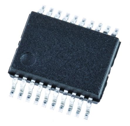
Image Preview
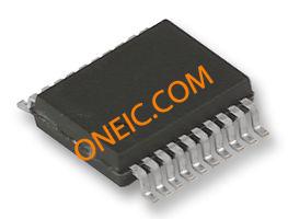
Image Preview