SN74ABT16373ADGGR
16-bit transparent D-type latches with 3-state outputs in 48-pin TSSOP
Manufacturer: ['rochester', 'analog-devices', 'ti']
series introduction
# Introduction to the SN74ABT16373ADGGR Product Series
## 1. Overview
The SN74ABT16373ADGGR belongs to the SN74ABT family of integrated circuits, which are widely recognized for their high - performance and reliability in digital logic applications. This particular product is a 16 - bit transparent D - type latch with 3 - state outputs. It is designed to meet the requirements of modern digital systems, offering efficient data storage and transfer capabilities.
## 2. Key Features
### 2.1 High - Speed Operation
One of the most significant features of the SN74ABT16373ADGGR is its high - speed performance. It is capable of operating at clock frequencies that can support the fast - paced data processing needs of contemporary digital systems. This high - speed operation is crucial for applications where real - time data handling is required, such as in high - speed data acquisition systems, communication interfaces, and advanced microprocessor - based systems.
### 2.2 3 - State Outputs
The 3 - state outputs of the SN74ABT16373ADGGR provide an additional level of flexibility in system design. In the high - impedance (Hi - Z) state, the outputs are effectively disconnected from the rest of the circuit. This feature allows multiple devices to share a common bus without interfering with each other. For example, in a multi - master bus system, different devices can be enabled or disabled as needed, ensuring that only one device is driving the bus at a time.
### 2.3 Transparent Latch Functionality
The transparent D - type latch design means that the output follows the input when the latch enable (LE) input is high. When the LE input goes low, the data present at the input is latched, and the output retains that value until the LE input goes high again. This functionality is useful for storing intermediate data values during the operation of a digital system, such as in a data buffer or a register file.
### 2.4 Wide Operating Voltage Range
The SN74ABT16373ADGGR can operate over a relatively wide voltage range. This allows it to be used in a variety of power supply environments, making it suitable for different types of digital systems. The ability to work with different voltage levels also provides some level of compatibility with other components in the system.
## 3. Technical Specifications
### 3.1 Electrical Characteristics
- **Supply Voltage (VCC)**: Typically operates within a range of 4.5V to 5.5V, which is common for many TTL - compatible digital circuits.
- **Input Voltage Levels**: The input high (VIH) and input low (VIL) voltage levels are defined to ensure proper logic level detection. For example, VIH is typically around 2V, and VIL is around 0.8V.
- **Output Voltage Levels**: The output high (VOH) and output low (VOL) voltage levels are designed to drive other digital components effectively. VOH is usually close to the supply voltage, and VOL is close to ground.
### 3.2 Timing Characteristics
- **Propagation Delay**: The propagation delay from the input to the output is an important parameter for high - speed applications. The SN74ABT16373ADGGR has relatively short propagation delays, which ensures that the data is transferred quickly and accurately through the latch.
- **Setup and Hold Times**: These times define the requirements for the input data to be stable before and after the active edge of the latch enable signal. Meeting these setup and hold times is essential for reliable data latching.
## 4. Package and Pin Configuration
### 4.
Images for reference

48-TSSOP
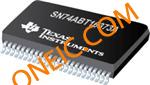
Image Preview
Image Preview